
High efficiency solid-state light source and methods of use and manufacture

a solid-state light source, high-efficiency technology, applied in the direction of boring tools, optical radiation measurement, dental tools, etc., can solve the problems of reducing the efficiency and duration of conventional high-intensity light sources, reducing the efficiency of conventional light sources for these applications, and only providing the spectral range required by the process, etc., to achieve the effect of eliminating the need for intricate optical coupling mechanisms, optimizing light output, and high efficiency

Active Publication Date: 2012-06-05
SILICON VALLEY BANK
View PDF300 Cites 124 Cited by
  • Summary
  • Abstract
  • Description
  • Claims
  • Application Information

AI Technical Summary

Benefits of technology

"The present invention provides a solid-state light source that can be used in various applications requiring high power density output. It is a unique array of solid-state light emitters that can produce high-intensity power output that previously required inefficient high-intensity lamps and / or expensive and complex laser devices. The device can produce power densities greater than about (50 mW / cm2 for any application requiring such power density. It can be configured differently for different applications, such as optical power output density, wavelength, optics, drive circuitry, and heat transfer. The device is self-contained, eliminating the need for intricate optical coupling mechanisms required by many prior art devices. It optimizes light output and is advantageous in the design of small cost effective LED projector systems."

Problems solved by technology

Unfortunately, conventional high-intensity light sources have a variety of disadvantages, as illustrated in the following examples.
The efficiency and duration of conventional light sources for these applications is extremely low.
For instance, 8000 W ultraviolet lamp sources (after filtering) are used in exposure of polymer resists, but they provide only 70 W of power in the spectral range required by the process.
None of the prior art discloses a semiconductor light source that can be adapted for a variety of applications and / or provide the high power densities required by a variety of applications.

Method used


Image

  • High efficiency solid-state light source and methods of use and manufacture
  • High efficiency solid-state light source and methods of use and manufacture
  • High efficiency solid-state light source and methods of use and manufacture

Examples


Embodiment Construction

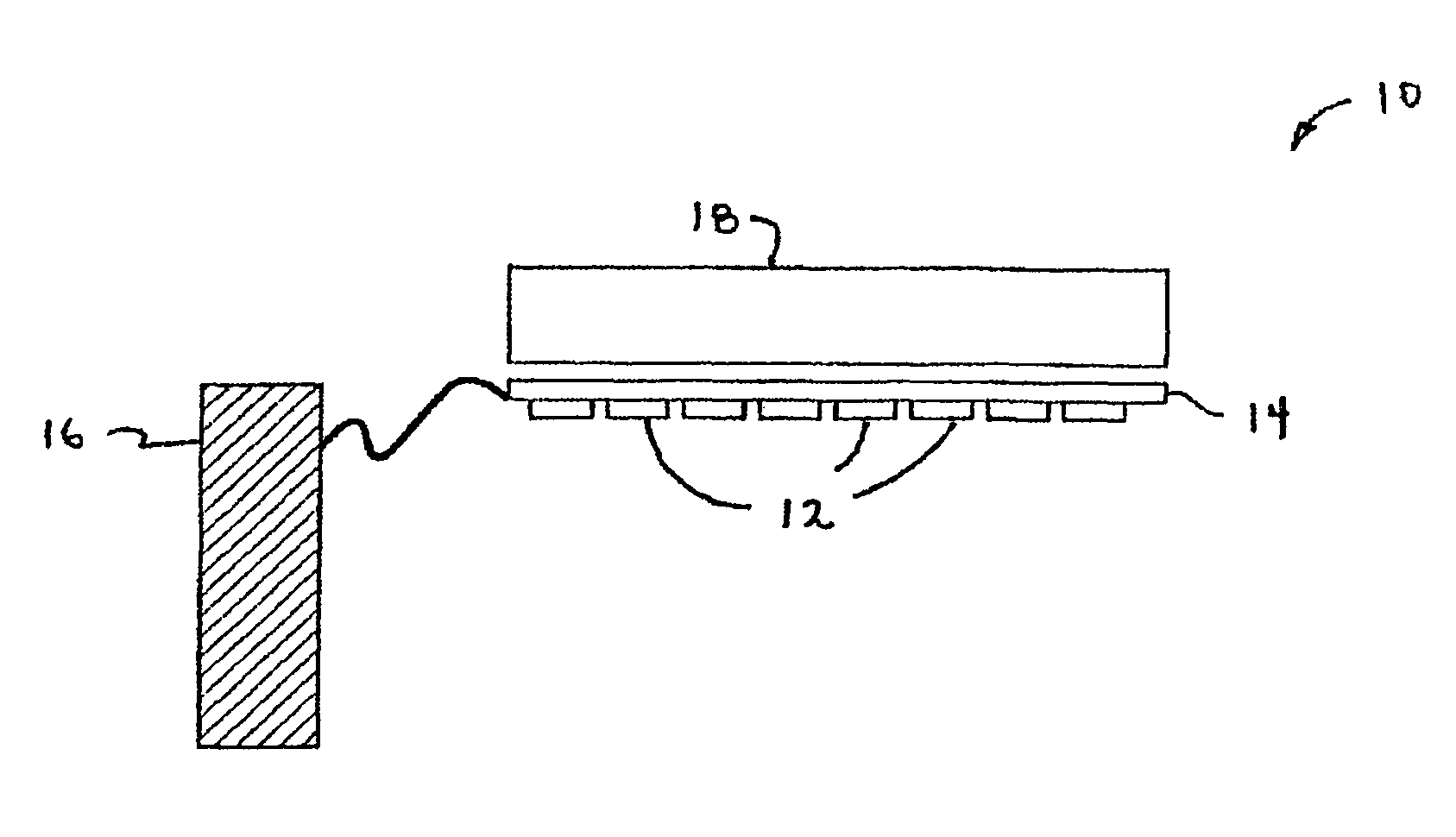
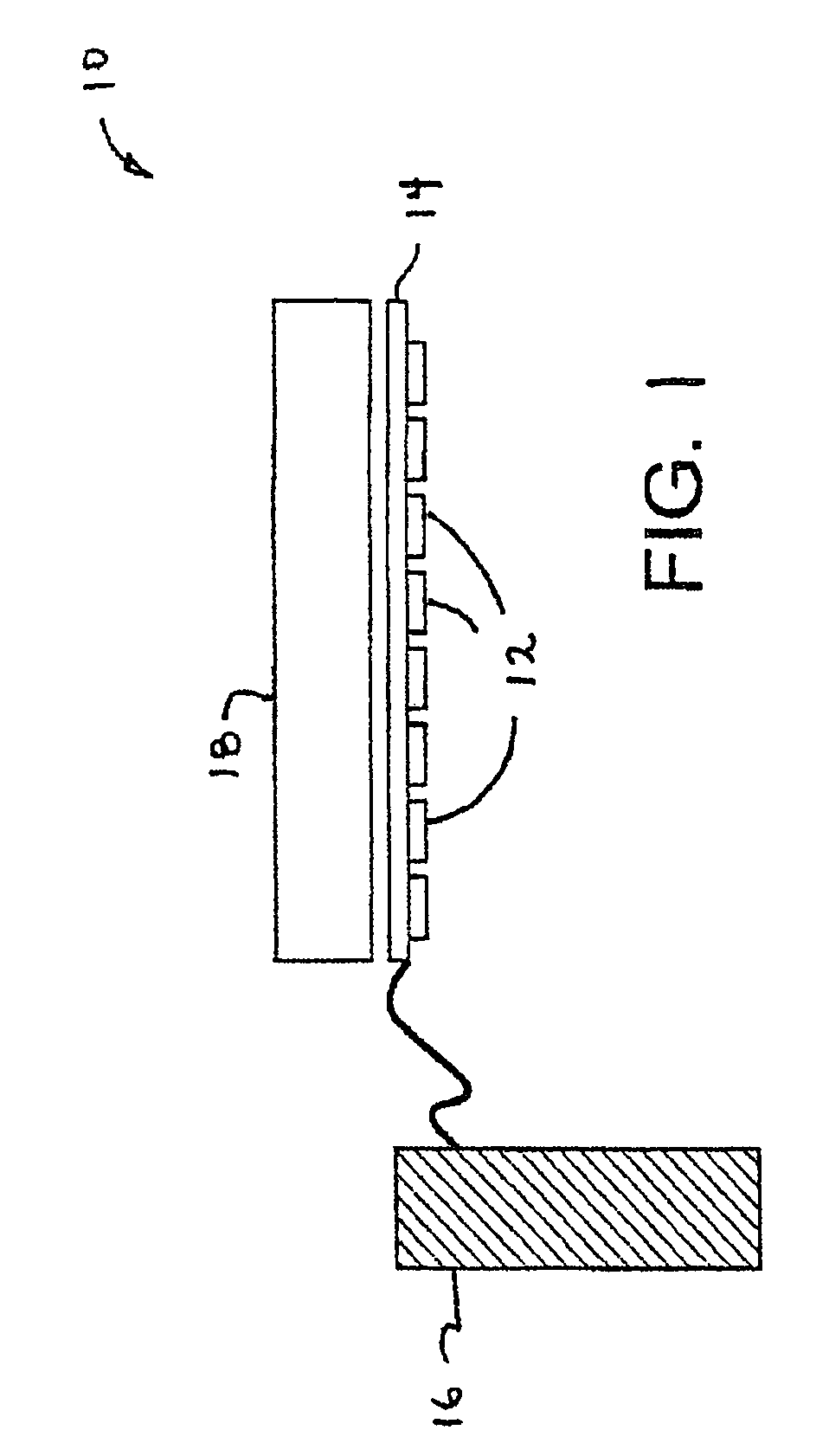
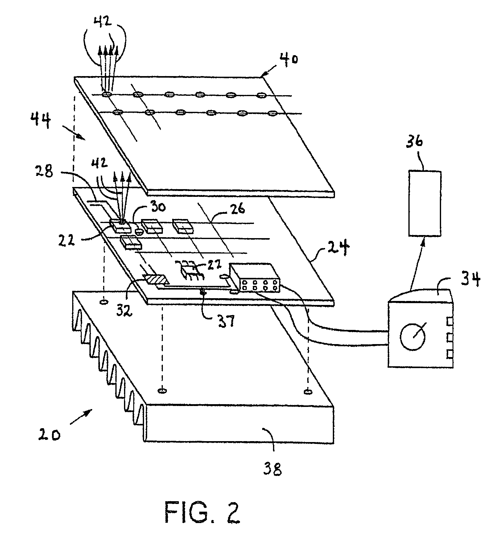
[0029]The present invention provides a lighting module that serves as a solid-state light source capable of performing operations in a variety of applications requiring high density power output. The device of the present invention includes a dense chip-on-board array of solid-state light emitters that produce high-intensity power output and further includes heat transfer; drive circuitry, light intensity, spectral purity, spatial uniformity, and directionality required for a variety of applications. Such applications are typically those requiring a power density output of over about 50 mW / cm2. Most applications typically require between about 50 mW / cm2 and 6,000 mW / cm2 and the present invention can provide power output in this range. However, it is contemplated that the lighting module of the present invention may be utilized in applications requiring a power density output greater than about 6,000 mW / cm2 Applications requiring power density output of between about 50 mW / cm2 and 6,...


PUM

PropertyMeasurementUnit
light wavelengthsaaaaaaaaaa
optimal wavelengthaaaaaaaaaa

Abstract

A high-intensity light source is formed by a micro array of a semiconductor light source such as a LEDs, laser diodes, or VCSEL placed densely on a liquid or gas cooled thermally conductive substrate. The semiconductor devices are typically attached by a joining process to electrically conductive patterns on the substrate, and driven by a microprocessor controlled power supply. An optic element is placed over the micro array to achieve improved directionality, intensity, and / or spectral purity of the output beam. The light module may be used for such processes as, for example, fluorescence, inspection and measurement, photopolymerzation, ionization, sterilization, debris removal, and other photochemical processes.

Description

[0001]This application is a Continuation-in-Part application claiming the benefit of PCT Application No. PCT / US03 / 14625 entitled “HIGH EFFICIENCY SOLID-STATE LIGHT SOURCE AND METHODS OF USE AND MANUFACTURE,” filed May 8, 2003, the entire disclosure of which is hereby incorporated by reference as if set forth in its entirety for all purposes.TECHNICAL FIELD[0002]This invention is generally directed to a solid-state light source having an electromagnetic radiation density sufficient to perform a variety of functions in a variety of production applications.BACKGROUND OF THE INVENTION[0003]High intensity pressure arc lamps of various varieties (for example, metal halide, mercury, Xenon, Excimer, and halogen) and other high-intensity light sources are used in the majority of commercial and industrial applications involving, for example, projection, illumination and displays, inspection, initiation of chemical or biological processes, image reproduction, fluorescence, exposure, sterilizat...

Claims


Application Information

Patent Timeline
Patent Type & Authority Patents(United States)
IPC IPC(8): F21V29/00A61L2/10A61L2/26A61L9/20F21K99/00G01N21/88G03F7/20H01L21/00H01L25/075H01L31/12H01L33/64H01S5/022H01S5/40
CPCA61L2/10A61L2/26A61L9/20F21K9/00G01N21/8806G03F7/7005C02F1/325H05B37/02H01L2924/0002A61L2202/14A61L2202/17H01L25/0753H01L33/64H01L2924/00H05B47/165H05B47/10F21V29/00F21V29/56F21V29/57F21V29/673A61L2/0047B41F23/0409B41F23/0453
Inventor OWENMCNEILVLACH, FRANCOIS
Owner SILICON VALLEY BANK
Learn More