Method for fabricating thin film transistor

a thin film transistor and transistor technology, applied in the direction of basic electric elements, electrical equipment, semiconductor devices, etc., can solve the problems affecting the element characteristics of tfts, and achieve the effect of improving the element characteristics of

Inactive Publication Date: 2012-07-17
TAIWAN TFT LCD ASSOC +5
View PDF22 Cites 2 Cited by
  • Summary
  • Abstract
  • Description
  • Claims
  • Application Information

AI Technical Summary

Benefits of technology

[0008]Accordingly, the present invention is directed to a method for fabricating a TFT, in which a photoresist layer is covered on a metal oxide active layer, so as to protect the metal oxide active layer.
[0014]The TFT formed by the method for fabricating a TFT of the present invention includes a photoresist layer, an insulating layer, or a protective layer covering the metal oxide active layer. Thus, the metal oxide active layer may be protected from being exposed to plasma, etchant, stripper, and other materials in the subsequent processes, so as to stabilize the thin film characteristics of the metal oxide active layer, thereby improving the element characteristics of the TFT.

Problems solved by technology

However, for example, for the TFT using ZnO as the active layer, in the subsequent process of forming a source and a drain, ZnO is easily damaged by, for example, plasma, etchant, stripper, and other materials, such that the active layer of the thin film characteristics would be changed, thereby influencing the element characteristics of the TFTs.

Method used


Image

  • Method for fabricating thin film transistor
  • Method for fabricating thin film transistor
  • Method for fabricating thin film transistor

Examples


first embodiment

The First Embodiment

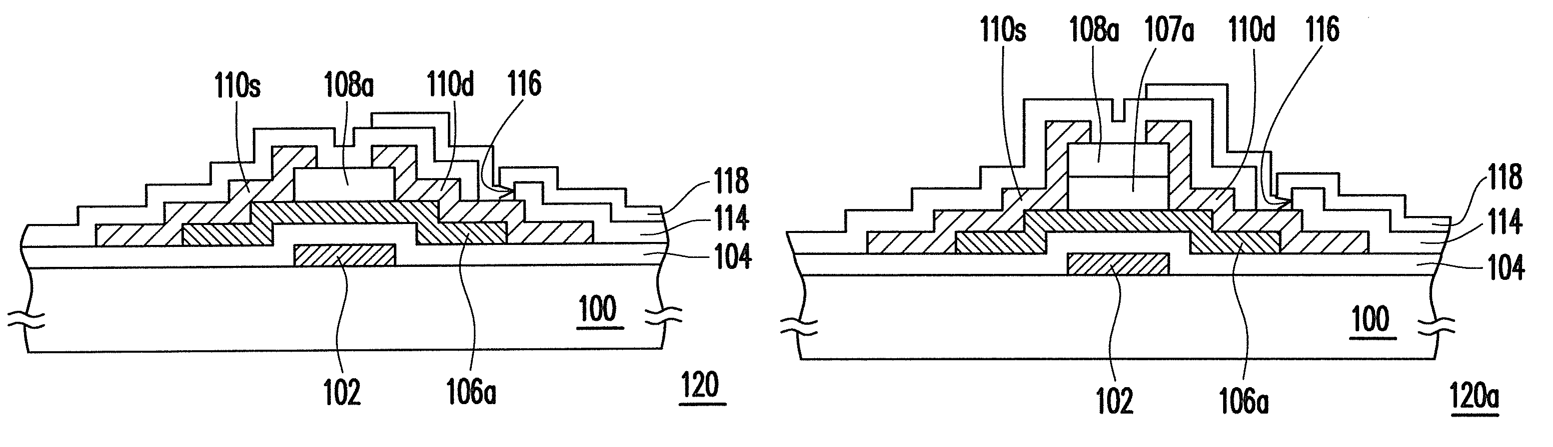
[0023]FIGS. 1A to 1G are schematic cross-sectional views illustrating processes of a method for fabricating a TFT according to a first embodiment of the present invention.

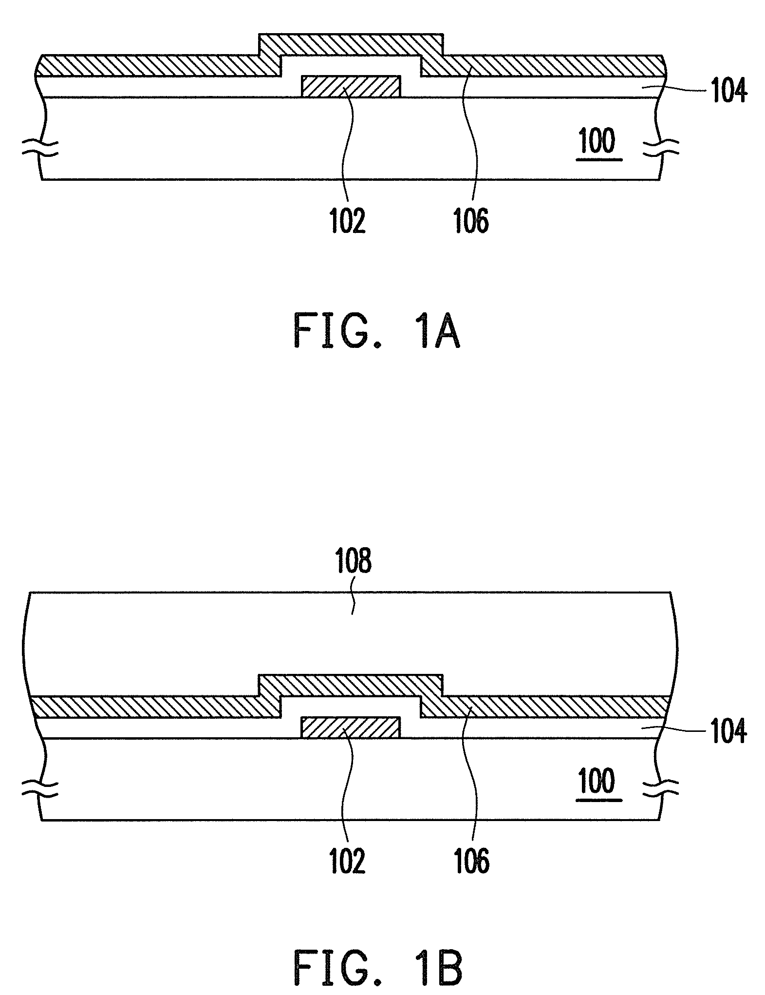
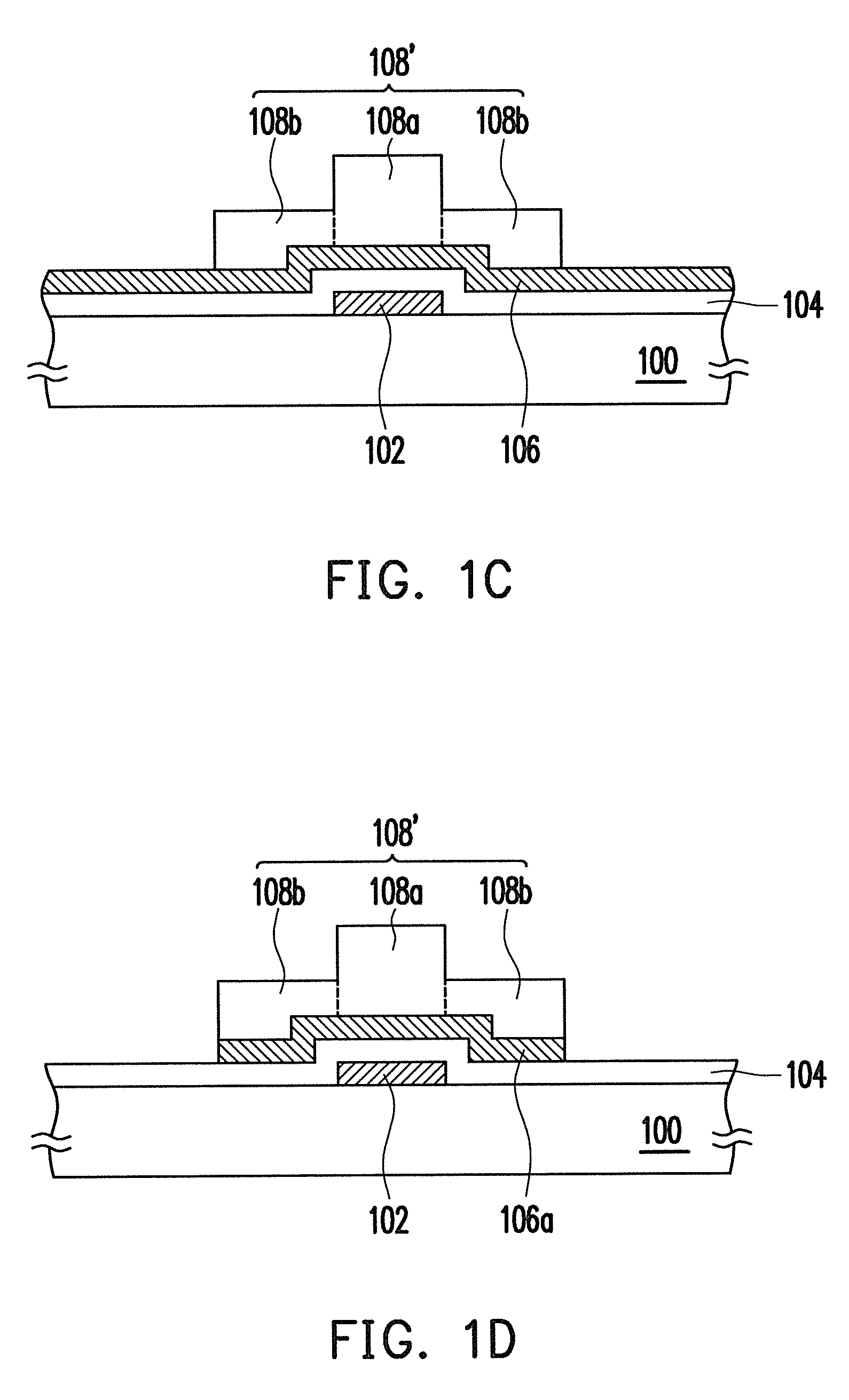
[0024]Referring to FIG. 1A, first, a gate 102 is formed on a substrate 100. The substrate 100 is, for example, a glass substrate, a quartz substrate, or other substrates. A material of the gate 102 is, for example, aluminum, chromium, tantalum, or other metal materials, and the forming method includes a thin film deposition process, a photolithography process, and an etching process. The thin film deposition process may be sputtering, electroplating, spin coating, printing, electroless plating, or other appropriate methods.

[0025]Then, a gate insulating layer 104 is formed on the substrate 100 to cover the gate 102. A material of the gate insulating layer 104 is, for example, silicon dioxide, silicon nitride, silicon oxynitride, or other dielectric materials, and the forming method is, for exampl...

second embodiment

The Second Embodiment

[0034]FIGS. 2A to 2G are schematic cross-sectional views illustrating processes of a method for fabricating the TFT according to a second embodiment of the present invention. In this embodiment, the forepart of the process of fabricating the TFT is similar to that of the first embodiment with reference to FIG. 1A and the corresponding illustrations, and the details will not be described herein again.

[0035]Referring to FIG. 2A, a gate 102, a gate insulating layer 104, and a metal oxide material layer 106 are already formed on a substrate 100. First, an insulating material layer 107 is formed on the metal oxide material layer 106. A material of the insulating material layer 107 includes an inorganic insulating material or an organic insulating material. The inorganic insulating material is, for example, silicon dioxide, silicon nitride, or other materials, the organic insulating material is, for example, polymethyl methacrylate (PMMA), polyvinyl phenol (PVP), or o...

third embodiment

The Third Embodiment

[0044]FIGS. 4A to 4D are schematic cross-sectional views illustrating processes of a method for fabricating the TFT according to a third embodiment of the present invention.

[0045]Referring to FIG. 4A, first, a gate 202 and a gate insulating layer 204 are formed in sequence on a substrate 200. The materials and forming methods of the gate 202 and the gate insulating layer 204 are similar to the first embodiment, and the details will not be described herein again.

[0046]Then, a metal oxide active layer 206 is formed on the gate insulating layer 204 above the gate 202. A material of the metal oxide active layer 206 includes a group II-VI compound, for example, ZnO, and the forming method is, for example, a non-vacuum process, which is the process performed in a non-vacuum chamber, for example, spin-coating, inject-printing, drop printing, casting, micro-stamping, screen-printing, imprinting, and other methods. In an embodiment, the method for forming the metal oxide ...


PUM

PropertyMeasurementUnit
thicknessaaaaaaaaaa
photosensitiveaaaaaaaaaa
non-photosensitiveaaaaaaaaaa

Abstract

A method for fabricating a thin film transistor is provided. A gate is formed on a substrate. A gate insulating layer is formed on the substrate to cover the gate. A metal oxide material layer is formed on the gate insulating layer. A photoresist layer is formed on the metal oxide material layer, in which a thickness of the photoresist layer above the gate is larger than that of the photoresist layer above two sides adjacent to the gate. A portion of the metal oxide material layer is removed to form a metal oxide active layer by using the photoresist layer as a mask. The photoresist layer above the two sides adjacent to the gate is removed and the remaining photoresist layer covers a portion of the metal oxide active layer. A source and a drain are formed on the metal oxide active layer covered by the photoresist layer.

Description

CROSS-REFERENCE TO RELATED APPLICATION[0001]This application claims the priority benefit of Taiwan application serial no. 97121565, filed on Jun. 10, 2008. The entirety of the above-mentioned patent application is hereby incorporated by reference herein and made a part of this specification.BACKGROUND OF THE INVENTION[0002]1. Field of the Invention[0003]The present invention generally relates to a method for fabricating a thin film transistor (TFT), in particular, to a method for fabricating a TFT using a metal oxide as an active layer.[0004]2. Description of Related Art[0005]In recent years, due to the progress of the semiconductor process technology, TFTs are fabricated more easily and quickly. The TFTs are widely applied to computer chips, mobile phone chips, TFT liquid crystal displays (TFT LCDs), or other electronic products. For example, for the TFT LCDs, the TFTs are used as charging or discharging switches of a storage capacitor.[0006]Generally speaking, according to materia...

Claims


Application Information

Patent Timeline
Patent Type & Authority Patents(United States)
IPC IPC(8): H01L21/00
CPCH01L29/7869
Inventor LUO, FANG-CHENLIANG, SHUO-WEICHIANG, SHIN-CHUANCHEN, CHAO-NANYU, CHIN-CHIH
Owner TAIWAN TFT LCD ASSOC
Why Eureka
Try Eureka