Method of fabricating a stacked oxide material for thin film transistor

a thin film transistor and oxide material technology, applied in the direction of semiconductor devices, basic electric elements, electrical appliances, etc., can solve the problems of difficult melting of silicon carbide, inability to manufacture silicon carbide by a high-productivity method, and defects called micropipes, etc., to achieve high withstandance, increase purity, and facilitate operation

Active Publication Date: 2013-02-05
SEMICON ENERGY LAB CO LTD
View PDF147 Cites 77 Cited by
  • Summary
  • Abstract
  • Description
  • Claims
  • Application Information

AI Technical Summary

Benefits of technology

[0007]In the case of a transistor used in a semiconductor device for high power application, characteristics such as high withstand voltage, high conversion efficiency, and high-speed switching are needed. Silicon is used for a semiconductor material of such a semiconductor device; however, from the above-described point of view, a novel semiconductor material which can further improve the characteristics is required.
[0008]As an example of a semiconductor material which can improve the above characteristics, silicon carbide can be given. Since silicon carbide has a small interatomic distance of approximately 0.18 nm in a Si—C bond, a high bond energy, and a large band gap which is about three times that of silicon, it is known that silicon carbide is advantageous in increasing the withstand voltage of a semiconductor device, reducing a loss of electric power, and the like.
[0017]Note that in the case where the first oxide semiconductor film having crystallinity and the second oxide semiconductor film having crystallinity contain In, in their flat-plate-shaped polycrystalline region, mobility is increased because electron clouds of In overlap with each other to be connected to each other. Therefore, high field-effect mobility can be realized in a transistor which includes an oxide semiconductor film having a polycrystalline region in a channel.
[0023]By using such a highly purified stacked body of an oxide semiconductor in a channel formation region of a transistor, a channel can be formed not only at a surface of the stacked body of an oxide semiconductor which is in contact with a gate insulating film but also the inside portion of the stacked body of an oxide semiconductor, i.e., a channel can be formed in the whole stacked body of an oxide semiconductor; thus, a large amount of current can flow in the transistor in an on state. When the transistor is in an off state, a depletion layer spreads to a deeper region inside the stacked body of an oxide semiconductor, whereby off-state current that is current flowing in a transistor in an off state can be reduced. Further, withstand voltage becomes higher and hot-carrier degradation is suppressed so that a semiconductor device for high power application to which a high voltage is applied can be manufactured.
[0024]By using such a highly purified stacked body of an oxide semiconductor in a diode, the diode has high rectification property.
[0026]According to one embodiment of the present invention, by using an oxide semiconductor film in which hydrogen concentration is reduced and the purity is increased and which has a polycrystalline region, a transistor and a diode can operate favorably. In a transistor, particularly, withstand voltage can be higher, a short channel effect can be reduced, and a high on-off ratio can be obtained. Therefore, a semiconductor device for high power application can be manufactured by using this transistor.

Problems solved by technology

However, it is difficult to melt silicon carbide because of its characteristics; therefore, silicon carbide cannot be manufactured by a method having high productivity such as a Czochralski (CZ) method or the like which is used for manufacturing a silicon wafer.
Moreover, there is also a problem in that silicon carbide has defects called micropipes.
Because of these problems, commercialization of a semiconductor device using silicon carbide is delayed.

Method used


Image

  • Method of fabricating a stacked oxide material for thin film transistor
  • Method of fabricating a stacked oxide material for thin film transistor
  • Method of fabricating a stacked oxide material for thin film transistor

Examples


embodiment 1

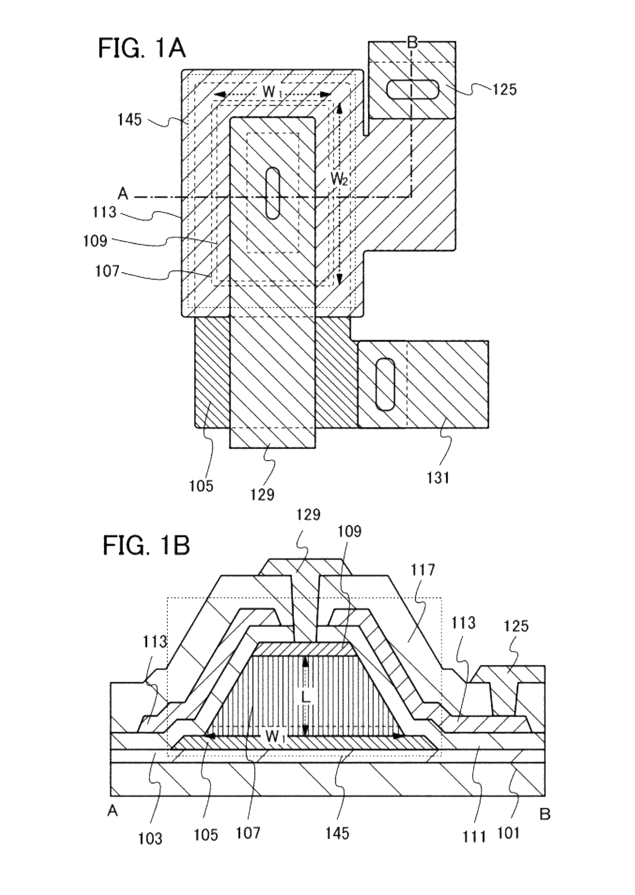
[0052]In this embodiment, a structure of a transistor, which is an embodiment of a semiconductor element, will be described with reference to FIGS. 1A and 1B.

[0053]FIG. 1A is a top view of a transistor 145, and FIG. 1B corresponds to a cross-sectional view taken along dashed line A-B in FIG. 1A.

[0054]As illustrated in FIG. 1B, a first electrode 105, an oxide semiconductor film 107 which has a polycrystalline region, and a second electrode 109 are stacked over an insulating film 103 formed over a substrate 101. Note that the second electrode 109 is stacked over and in contact with the entire top surface of the oxide semiconductor film 107. A gate insulating film 111 is provided so as to cover the first electrode 105, the oxide semiconductor film 107, and the second electrode 109. Over the gate insulating film 111, a third electrode 113 facing at least a side surface of the oxide semiconductor film is provided. An insulating film 117 functioning as an interlayer insulating film is pro...

embodiment 2

[0138]In this embodiment, a transistor having a structure different from that of Embodiment 1 will be described with reference to FIGS. 7A and 7B.

[0139]FIG. 7A is a top view of a transistor 147, and FIG. 7B corresponds to a cross-sectional view taken along dashed line A-B in FIG. 7A.

[0140]As illustrated in FIG. 7B, the first electrode 105, the oxide semiconductor film 107, and the second electrode 109 are stacked over the insulating film 103 formed over the substrate 101. Note that this structure is different from that in Embodiment 1 in that the periphery of the second electrode 109 is inside the periphery of the oxide semiconductor film 107. The gate insulating film 111 is provided so as to cover the first electrode 105, the oxide semiconductor film 107, and the second electrode 109. Over the gate insulating film 111, the third electrode 113 is provided so as to face at least side surfaces of the oxide semiconductor film and the second electrode. The insulating film 117 functionin...

embodiment 3

[0146]In this embodiment, a structure of a three-terminal type diode which is manufactured using the transistor described in Embodiment 1 or 2 will be described with reference to FIGS. 8A and 8B.

[0147]FIGS. 8A and 8B are each a cross-sectional view of a three-terminal type diode.

[0148]In a three-terminal type diode 149a illustrated in FIG. 8A, the first electrode 105, the oxide semiconductor film 107, and the second electrode 109 are stacked over the insulating film 103 formed over the substrate 101. The gate insulating film 111 is provided so as to cover the first electrode 105, the oxide semiconductor film 107, and the second electrode 109. The third electrode 113 is provided over the gate insulating film 111. Further, an opening is formed in the gate insulating film 111 and the second electrode 109 and the third electrode 113 are connected to each other through the opening.

[0149]In a three-terminal type diode 149b illustrated in FIG. 8B, the first electrode 105, the oxide semicon...


PUM


Abstract

Objects are to provide a semiconductor device for high power application in which a novel semiconductor material having high productivity is used and to provide a semiconductor device having a novel structure in which a novel semiconductor material is used. The present invention is a vertical transistor and a vertical diode each of which has a stacked body of an oxide semiconductor in which a first oxide semiconductor film having crystallinity and a second oxide semiconductor film having crystallinity are stacked. An impurity serving as an electron donor (donor) which is contained in the stacked body of an oxide semiconductor is removed in a step of crystal growth; therefore, the stacked body of an oxide semiconductor is highly purified and is an intrinsic semiconductor or a substantially intrinsic semiconductor whose carrier density is low. The stacked body of an oxide semiconductor has a wider band gap than a silicon semiconductor.

Description

TECHNICAL FIELD[0001]The present invention relates to a semiconductor device which has a semiconductor element using an oxide semiconductor and a manufacturing method of the semiconductor device.BACKGROUND ART[0002]A technique of forming a thin film transistor (TFT) by using a thin semiconductor film formed at a relatively low temperature over a substrate having an insulating surface has attracted attention. A thin film transistor is used for a display device typified by a liquid crystal television. A silicon-based semiconductor material is known as a material for a semiconductor thin film applicable to a thin film transistor. Other than a silicon-based semiconductor material, an oxide semiconductor has attracted attention.[0003]As a material for the oxide semiconductor, zinc oxide and a material containing zinc oxide as its component are known. Further, a thin film transistor formed using an amorphous oxide (an oxide semiconductor) having an electron carrier density lower than 1018...

Claims


Application Information

Patent Timeline
Patent Type & Authority Patents(United States)
IPC IPC(8): H01L21/00H01L29/66
CPCH01L21/02472H01L21/02483H01L21/02554H01L21/02565H01L21/02631H01L21/02634H01L29/78693H01L29/045H01L29/66666H01L29/78642H01L29/7869H01L29/247H01L29/66969H01L21/02667H01L29/06H01L29/66742H01L27/1225H01L33/305
Inventor YAMAZAKI, SHUNPEI
Owner SEMICON ENERGY LAB CO LTD
Why Eureka
Try Eureka