Method of manufacturing SOI substrate

a technology of soi substrate and manufacturing method, which is applied in the direction of semiconductor/solid-state device manufacturing, basic electric elements, electric apparatus, etc., can solve the problem of preventing productivity improvement, and achieve the effect of efficient reprocessing

Inactive Publication Date: 2013-02-19
SEMICON ENERGY LAB CO LTD
View PDF7 Cites 2 Cited by
  • Summary
  • Abstract
  • Description
  • Claims
  • Application Information

AI Technical Summary

Benefits of technology

[0009]In the case of utilizing the hydrogen ion implantation separation method, the volume of a microbubble layer formed in a silicon wafer is changed by a heat treatment and a split occurs at the microbubble layer, so that an SOI substrate can be obtained. However, the semiconductor layer of the SOI substrate after the split has a rough surface due to the microbubble layer, and thus needs to be subjected to a planarization treatment. A chemical mechanical polishing (CMP) treatment can be employed to planarize the surface of the semiconductor layer (or the silicon wafer after the split). However, in a CMP treatment, the amount of polishing of the semiconductor layer (or the silicon wafer) tends to be large and therefore productivity is prevented from improving and the manufacturing cost is prevented from reducing.
[0010]In view of the above problem, an object of an embodiment of the present invention is to manufacture an SOI substrate in which a surface of a semiconductor layer is efficiently planarized. Further, an object of the present invention is to provide a semiconductor device using the SOI substrate. Further, an object of an embodiment of the present invention is to efficiently reprocess a bond substrate.
[0016]According to an embodiment of the present invention, an SOI substrate in which a surface of a semiconductor layer is efficiently planarized can be provided. Further, a semiconductor device using the SOI substrate can be provided. Further, a bond substrate can be efficiently reprocessed.

Problems solved by technology

However, the semiconductor layer of the SOI substrate after the split has a rough surface due to the microbubble layer, and thus needs to be subjected to a planarization treatment.
However, in a CMP treatment, the amount of polishing of the semiconductor layer (or the silicon wafer) tends to be large and therefore productivity is prevented from improving and the manufacturing cost is prevented from reducing.

Method used


Image

  • Method of manufacturing SOI substrate
  • Method of manufacturing SOI substrate
  • Method of manufacturing SOI substrate

Examples


embodiment 1

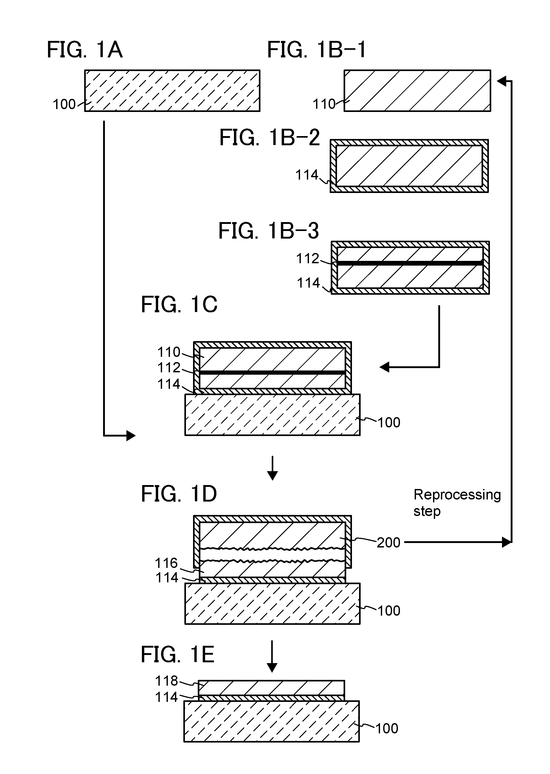
[0030]In this embodiment, an example of a method for manufacturing an SOI substrate is described with reference to FIGS. 1A, 1B-1 to 1B-3, 1C, 1D, and 1E and FIG. 2.

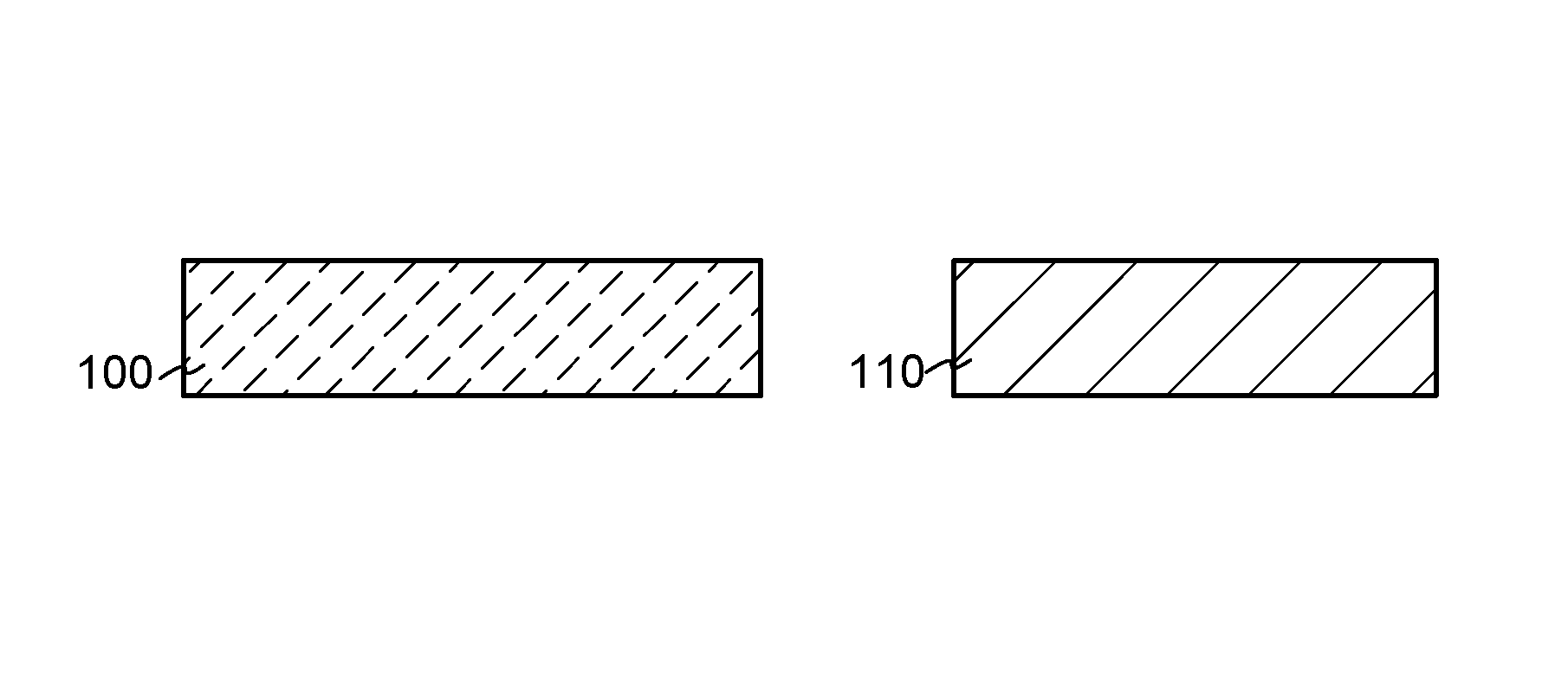
[0031]First, a base substrate 100 is prepared (see FIG. 1A). As the base substrate 100, it is possible to use a light-transmitting glass substrate used for a liquid crystal display device or the like. As the glass substrate, a substrate having a strain point of 580° C. or higher (preferably 600° C. or higher) may preferably be used. Further, the glass substrate is preferably a non-alkali glass substrate. The non-alkali glass substrate is formed using a glass material such as aluminosilicate glass, aluminoborosilicate glass, or barium borosilicate glass, for instance.

[0032]Note that as the base substrate 100, it is possible to use an insulating substrate such as a ceramic substrate, a quartz substrate, or a sapphire substrate, a substrate formed of a semiconductor such as silicon, a substrate formed of a conductor such as...

embodiment 2

[0075]In this embodiment, another example of a manufacturing method of an SOI substrate is described with reference to FIGS. 3A-1, 3A-2, 3B-1 to 3B-3, 3C, 3D, and 3E. This embodiment is different from Embodiment 1 in that an insulating layer 101 is formed over a base substrate. Therefore, this point is mainly described below.

[0076]First, the base substrate 100 is prepared (see FIG. 3A-1), and the insulating layer 101 is formed over the base substrate (see FIG. 3A-2). Refer to FIG. 1A for the base substrate 100.

[0077]There is no particular limitation on the method for forming the insulating layer 101, to which a sputtering method, a plasma CVD method, or the like can be applied, for example. Since the insulating layer 101 has a surface for bond, the insulating layer 101 is preferably formed such that this surface has high planarity. The insulating layer 101 can be formed using one or more materials selected from a silicon oxide, a silicon nitride, a silicon oxynitride, a silicon nitr...

embodiment 3

[0098]In this embodiment, a manufacturing method of a semiconductor device using the SOI substrate according to the aforementioned embodiment will be described with reference to FIGS. 4A to 4E and FIGS. 5A to 5D. In this embodiment, a manufacturing method of a semiconductor device including a plurality of transistors will be described as an example of the semiconductor device. Various semiconductor devices can be formed with the use of transistors described below in combination.

[0099]FIG. 4A is a cross-sectional view illustrating a part of the SOI substrate manufactured using the method described in aforementioned embodiment.

[0100]The semiconductor layer 118 corresponds to the semiconductor layer 118 in FIG. 3E and has a surface whose planarity is improved.

[0101]In order to control the threshold voltage of the transistor, a p-type impurity element such as boron, aluminum, or gallium, or an n-type impurity element such as phosphorus or arsenic may be added to the semiconductor layer ...


PUM


Abstract

An object of the present invention is to provide an SOI substrate including a semiconductor layer which is efficiently planarized. A method for manufacturing an SOI substrate includes a step of irradiating a bond substrate with an accelerated ion to form an embrittlement region; a step of bonding the bond substrate and the base substrate with an insulating layer positioned therebetween; a step of splitting the bond substrate at the embrittlement region to leave a semiconductor layer bonded to the base substrate; a step of disposing the semiconductor layer in front of a semiconductor target containing the same semiconductor material as the semiconductor layer; and a step of alternately irradiating the surface of the semiconductor layer and the semiconductor target with a rare gas ion, so that the surface of the semiconductor layer is planarized.

Description

BACKGROUND OF THE INVENTION[0001]1. Field of the Invention[0002]The present invention relates to a method for manufacturing a substrate over which a semiconductor layer is provided with an insulating layer positioned therebetween, and particularly relates to a method for manufacturing a silicon on insulator (SOI) substrate. Further, the present invention relates to a method for recycling a bond substrate in the manufacturing method of an SOI substrate.[0003]2. Description of the Related Art[0004]As substrates suitable for manufacture of semiconductor devices that achieve low power consumption and high-speed operation, attention has been directed to SOI substrates in which a semiconductor layer is provided over a base substrate having an insulating surface.[0005]One of known methods for manufacturing an SOI substrate is a hydrogen ion implantation separation method (see Patent Document 1). The hydrogen ion implantation separation method is a technique of forming an SOI substrate in t...

Claims


Application Information

Patent Timeline
Patent Type & Authority Patents(United States)
IPC IPC(8): H01L21/30
CPCH01L21/02046H01L21/02052H01L21/302H01L21/76254
Inventor YAMAZAKI, SHUNPEITAKAYAMA, TORUSATO, MIZUHOUTO, NORIAKI
Owner SEMICON ENERGY LAB CO LTD
Why Eureka
Try Eureka