Method and apparatus for laser singulation of brittle materials

a technology of brittle materials and laser singulation, which is applied in the direction of laser beam welding apparatus, manufacturing tools, welding/soldering/cutting articles, etc., can solve the problems of limiting the useful life of parts, device failure, and real estate, and achieve the effect of improving the strength of die breakag

Active Publication Date: 2013-02-26
ELECTRO SCI IND INC
View PDF17 Cites 12 Cited by
  • Summary
  • Abstract
  • Description
  • Claims
  • Application Information

AI Technical Summary

Benefits of technology

[0010]This invention is an improved method and apparatus for laser machining brittle materials. Aspects of this invention include providing a laser having laser parameters and making a first cut in the workpiece with the laser using first laser parameters, then making a second cut in the workpiece with the laser using second laser parameters, the second cut being adjacent to the first cut while avoiding the debris cloud created by the first laser cut. Aspects of this invention further include moving the point at which the laser intersects the workpiece in order to avoid the debris cloud created by the previous cut and then making a cut with a laser using second laser parameters. Aspects of this invention gain the advantages of laser processing, including increased throughput, smaller street sizes and reduced consumable cost, while eliminating problems associated with lasers such as the heat affected zone and re-deposit of debris, thereby increasing die break strength.
[0012]Aspects of this invention singulate substrates or wafers by first making a laser cut in the substrate or wafer. Laser parameters are adjusted to provide desired cutting speed and kerf size and shape. This laser cut is made partially through the wafer or substrate. The laser parameters associated with this cut are selected so as to minimize cracking and re-deposited debris. Lower fluence laser parameters increase cutting time but since this cut is only partially through the wafer or substrate the impact on system throughput is not great. Also note that these initial laser cuts may require multiple passes of the laser beam to make the cut to the depth desired or the laser beam may be directed to impinge on the substrate of wafer at various points while cutting.
[0013]Following the initial cut, aspects of this invention adjusting the laser parameters to increase the laser fluence at the surface of the wafer or substrate and then directing the laser beam to machine a through cut in the wafer or substrate adjacent to the previous cut. Laser parameters are adjusted to permit the laser beam to remove material from the wafer while minimizing additional damage to the wafer or substrate. This is because the debris cloud created by the laser pulses making the second cut has room to expand into the space made by the previous cut. In this way the debris cloud dissipates more rapidly permitting increased repetition rate pulsing with more energetic pulses which supports improved throughput while reducing cracking and re-deposited debris. This permits increased throughput with increased die break strength. Aspects of this invention can also process wafers or substrates in an iterative fashion, alternating first laser parameter cuts with second parameters cuts as the cuts go deeper into the wafer or substrate. Laser pulses are focused at increasing depths to permit machining deeper and deeper cuts into the material.
[0014]An advantage of processing substrates or wafers according to aspects of this invention is that the first cut processing can take place on the same laser processing system that makes the second cuts. The ESI Cignis Laser Singulation system that made the initial cuts is adapted to create the cut without causing additional damage to the substrate of wafer by modifying the laser parameters associated with the laser processing beam to permit the laser to remove material from the substrate of wafer without creating a HAZ or debris. This is possible because far less material is being removed per unit time, therefore the laser fluence can be lower. The system is also adapted to permit machining adjacent locations efficiently.
[0016]Advantages of these aspects of this invention are that the substrate or wafer does not have to be moved and re-aligned on a separate machine nor does it have to be flipped and put back into the machine for laser processing from a different side, nor does the machine have to be designed to process substrates or wafers from both sides. In addition, no chemicals or additional process steps such as depositing an additional layer of material on the wafer or substrate are required by aspects of this invention. While this requires at least two passes to process a single cut in a wafer or substrate, the number of passes are substantially less than approaches that skip adjacent locations rely on multiple passes. Processing wafers or substrates according to aspects of this invention improves die break strength and removes re-deposited material from singulated devices without requiring additional equipment, process steps or consumable supplies.

Problems solved by technology

Issues related to device singulation include real estate, device damage, cost, complexity and system throughput.
This HAZ should not be allowed to overlap the active device area or it may either cause part failures immediately or limit the useful life of the part.
The HAZ also can cause device failure from cracks or chips in the HAZ propagating from the HAZ to the active device area of the device as the device is used.
Another problem related to laser singulation of wafers or substrates is the re-deposit of material removed from the kerf.
Nearer the periphery of the beam or directly adjacent to the beam the material of the substrate may not receive enough energy to ablate the material but rather vaporizes or melts and boils the material.
If this debris reaches active circuit areas of the device it can cause undesirable electronic malfunctions and therefore must be removed prior to packaging the device.
In addition, debris re-deposited along the edge of the cut from materials vaporized or liquefied by the laser can cause damage to the circuit and reduce reliability.
The HAZ can cause a reduction in die break strength and the re-deposited debris can cause device failure.
Another issue with laser singulation of substrates or wafers is improving system throughput.
In particular, laser parameters which provide higher cutting speed also create more HAZ and re-deposited debris, which is undesirable.
It is also noted that laser parameters which provide high cutting speed also create a debris cloud at the cutting site.
This transferred energy and material causes cracking, deterioration of the feature sidewall and increased debris.
In addition, if more energetic pulses or more pulses are directed to the workpiece in an effort to transmit more energy through the debris cloud to the workpiece and thereby continue to machine material, more energy is coupled into the debris cloud making the cracking, deterioration and debris problems worse.
Even ultra fast processes which use short duration pulses in the picosecond or femtosecond range to ablate material before the material has time to transfer heat to adjacent regions cannot avoid coupling energy into the debris cloud.
This energy causes consequent damage to the workpiece depending upon the material and the laser parameters used.

Method used


Image

  • Method and apparatus for laser singulation of brittle materials
  • Method and apparatus for laser singulation of brittle materials
  • Method and apparatus for laser singulation of brittle materials

Examples


Embodiment Construction

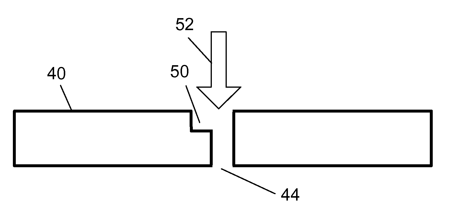
[0024]This invention is an improved method for laser singulation of electronic devices fabricated on a substrate or wafer. An embodiment of this invention includes a laser processing system having a laser having laser parameters. This embodiment uses this laser to make a partial cut in the substrate or wafer using a first set of laser parameters. These parameters allow the laser to make the desired cut in the wafer or substrate with an acceptable kerf width and at an acceptable rate without creating unacceptable HAZ or re-deposited debris. This embodiment then cuts the wafer or substrate with a laser using second set of laser parameters adjacent to the first cut. Making the second cut adjacent to the first cut allows the debris cloud from the substrate or wafer to being cut to dissipate into the volume of the first cut, thereby reducing the deleterious effects associated with heating the debris cloud with subsequent laser pulses. Workpieces machined in this fashion exhibit improved ...


PUM

PropertyMeasurementUnit
wavelengthaaaaaaaaaa
speedaaaaaaaaaa
spot sizeaaaaaaaaaa

Abstract

An improved method for singulation of electronic substrates into dice uses a laser to first form cuts in the substrate and then chamfers the edges of the cuts by altering the laser parameters. The chamfers increase die break strength by reducing the residual damage and removes debris caused by the initial laser cut without requiring additional process steps, additional equipment or consumable supplies.

Description

TECHNICAL FIELD[0001]The present invention relates to improved methods and apparatus for machining feature in brittle materials. In particular, it relates to improved methods and apparatus for machining of workpieces containing electronic devices in which multiple copies of a device are constructed on a common substrate. In more particular it relates to device singulation or the separation of semiconductor wafers into individual devices using a laser.BACKGROUND OF THE INVENTION[0002]Electronic devices are typically manufactured by producing multiple copies of the same device on a substrate or workpiece. In particular, semiconductor devices are manufactured on substrates referred to as wafers, which are thin disks of materials such as silicon, gallium arsenide or sapphire or other materials which are capable of supporting the various processes that create semiconductor devices. These devices at some point in the manufacturing process need to be separated into individual devices for s...

Claims


Application Information

Patent Timeline
Patent Type & Authority Patents(United States)
IPC IPC(8): B23K26/00
CPCB23K26/0042B23K26/0626B23K26/4075H01L21/78B23K26/0006B23K26/40B23K26/38B23K2103/50B23K2103/56H01L21/268
Inventor OSAKO, YASUFINN, DARAGH
Owner ELECTRO SCI IND INC
Why Eureka
Try Eureka