Method for cleaning the surface of a silicon substrate

a technology of silicon substrate and cleaning method, which is applied in the direction of cleaning using liquids, sustainable manufacturing/processing, and final product manufacturing, etc., can solve the problems of high fabrication cost and achieve the effect of reducing fabrication cos

Active Publication Date: 2013-03-26
TOTAL PUTEAUX FR
View PDF2 Cites 3 Cited by
  • Summary
  • Abstract
  • Description
  • Claims
  • Application Information

AI Technical Summary

Benefits of technology

[0007]Thus, the aim of the invention is to provide a method of cleaning the surface of a silicon substrate using a dry technique that can avoid the use of polluting liquid chemicals and reduce fabrication costs.

Problems solved by technology

However, the relatively large quantity of deionized water and chemicals used in those wet processes represents a major source of pollution and incurs high fabrication costs.

Method used


Image

  • Method for cleaning the surface of a silicon substrate
  • Method for cleaning the surface of a silicon substrate

Examples


Embodiment Construction

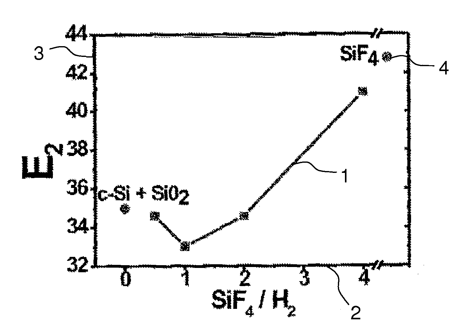
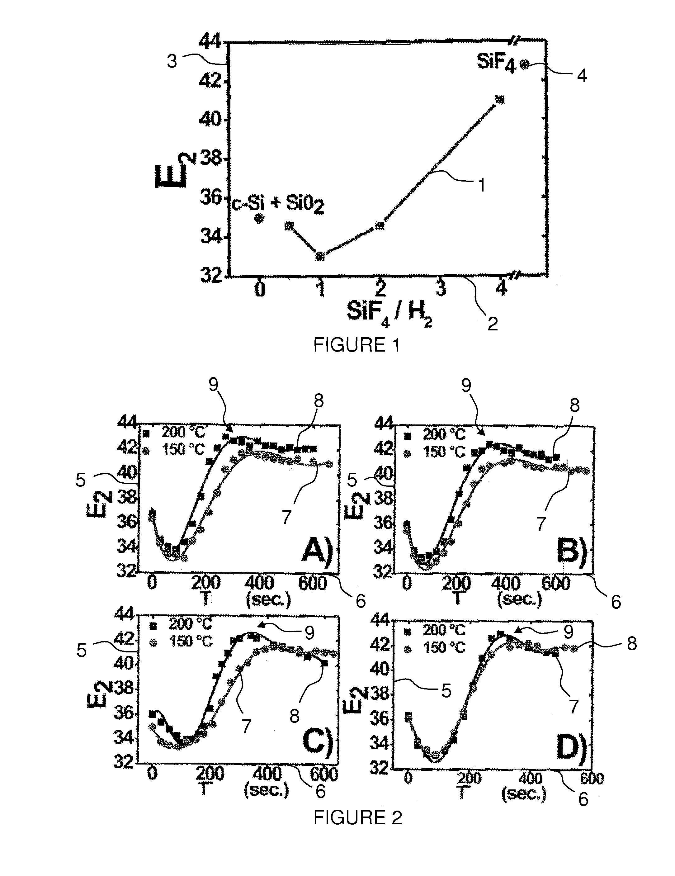
[0026]In one implementation of the invention, the method of cleaning the surface of a silicon substrate initially covered with a layer of native silicon oxide includes a step a) of exposing the surface to a radiofrequency plasma generated from a fluorinated gas in a reaction chamber, resulting in stripping the layer of silicon oxide by gas phase etching (dry technique).

[0027]A fluorinated gas is injected into the reaction chamber of a plasma enhanced chemical vapor deposition reactor (PECVD). The plasma excited by a radiofrequency voltage (RF) comprises fluorine-based elements (molecules, atoms, ions).

[0028]This step a) is carried out for a period in the range 60 s to 900 s. The power of the plasma is in the range 1 W to 30 W, corresponding to a power density in the range 10 mW / cm2 to 350 mW / cm2. The pressure of the fluorinated gas is in the range 10 mTorr to 200 mTorr.

[0029]The fluorinated (or fluorine-based) gas is preferably a SiF4 gas. Other fluorinated gases may be used such as...


PUM

PropertyMeasurementUnit
temperatureaaaaaaaaaa
poweraaaaaaaaaa
pressureaaaaaaaaaa

Abstract

A method for cleaning the surface of a silicon substrate, covered by a layer of silicon oxide includes: a) exposing the surface for 60 to 900 seconds to a radiofrequency plasma, generated from a fluorinated gas, to strip the silicon oxide layer and induce the adsorption of fluorinated elements on the substrate surface, the power density generated using the plasma being 10 mW/cm2 to 350 mW/cm2, the fluorinated gas pressure being 10 mTorrs to 200 mTorrs, and the substrate temperature being lower than or equal to 300° C.; and b) exposing the surface including the fluorinated elements for 5 to 120 seconds to a hydrogen radiofrequency plasma, to remove the fluorinated elements from the substrate surface, the power density generated using the plasma being 10 mW/cm2 to 350 mW/cm2, the hydrogen pressure being 10 mTorrs to 1 Torr, and the substrate temperature being lower than or equal to 300° C.

Description

FIELD OF THE INVENTION[0001]The invention relates to a method of cleaning the surface of a silicon substrate for the fabrication of a heterojunction solar cell.[0002]Crystalline silicon solar cells are widely used in the photovoltaics industry because of their high efficiencies.[0003]Heterojunction solar cells can be used to obtain high efficiencies (>22%) even for solar cells obtained from a very thin wafer of silicon (˜100 μm [micrometer]).BACKGROUND OF THE INVENTION[0004]It is known that after a step of texturizing the surface, silicon substrates undergo a wet chemical etching step to clean the surface of the silicon substrate, i.e. to remove the layer of silicon oxide (SiO2) that forms naturally on the surface of the substrate. That wet chemical method is known from the document by Karen Reinhardt and Werner Kern “Handbook of Semiconductor Wafer Cleaning Technology”, 2nd edition (2007).[0005]That wet chemical cleaning method requires the use of solutions such as those based o...

Claims


Application Information

Patent Timeline
Patent Type & Authority Patents(United States)
IPC IPC(8): C25F3/02
CPCC30B29/06H01L31/1804C30B33/12Y02E10/547Y02P70/50
Inventor ROCA I CABARROCAS, PEREMORENO, MARIO
Owner TOTAL PUTEAUX FR
Why Eureka
Try Eureka