
Electrophotographic photoconductor and manufacturing method thereof

a photoconductor and electrophotography technology, applied in the direction of electrographic process, instruments, corona discharge, etc., can solve the problems of solvent cracking, large cracks on the photosensitive layer, and the use of bisphenol z polycarbonate as a resin binder in the electrophotographic photoconductor was problematic, so as to improve the cracking resistance of solvents, improve the lubricity, and improve the effect of lubrication

Active Publication Date: 2013-03-26
FUJI ELECTRIC CO LTD
View PDF23 Cites 4 Cited by
  • Summary
  • Abstract
  • Description
  • Claims
  • Application Information

AI Technical Summary

Benefits of technology

The present invention relates to improving the performance of electrophotographic photoconductors by using a specific type of resin binder, called copolymer polyarylate resin. This resin has a high ratio of isophthalic acid structure, which increases its resistance to solvent cracking and allows for better solubility in solvents for coating solutions. The addition of alkylene groups in the resin molecule makes it more flexible and easier to form a stable coating. The resulting photoconductor has improved image quality and durability, and is more resistant to cracking when using certain types of resin.

Problems solved by technology

However, using a bisphenol Z polycarbonate as a resin binder in an electrophotographic photoconductor was problematic on account solvent cracking and the readiness with which sebum-derived cracks appeared in the photosensitive layer.
Solvent cracking is likely to occur due to contact with the solvent of cleaners that are used for cleaning the charging member or the photoconductor.
In particular, larger cracks appear on the photosensitive layer when, after cleaning of a contact charging-type charging roller, the solvent does not evaporate completely and remains in contact with the photoconductor.
In particular, solvent cracking occurs readily in liquid development processes, since in this case the carrier liquid in which the toner is dispersed comes into direct contact with the photoconductor.
To deal with the above problems, Patent Document 1 proposes, for instance, to use a mixture of a bisphenol A polycarbonate resin and a bisphenol Z polycarbonate resin, but this method has proved to be an insufficient solution.
The various polyester resins having a bisphenol structure proposed to date have fail to cope sufficiently with the issue of solvent cracking resistance.
However, such surface protective layers as well have failed to avoid the same problem of cracking that bedevils the photosensitive layer.

Method used


Image

  • Electrophotographic photoconductor and manufacturing method thereof
  • Electrophotographic photoconductor and manufacturing method thereof
  • Electrophotographic photoconductor and manufacturing method thereof

Examples


manufacturing example 1

Method for Manufacturing a Copolymer Polyarylate Resin (III-1)

[0051]A 5-liter 4-necked flask was charged with 300 mL of deionized water, 1.24 g of NaOH, 0.459 g of p-tert-butyl phenol, 30.3 g of bisphenol A, and 0.272 g of tetrabutylammonium bromide. Further, 9.261 g of terephthalic acid chloride, 17.704 g of isophthalic acid chloride and 0.246 g of adipic acid chloride were dissolved in 300 mL of methylene chloride. The resulting solution was added over 2 minutes, and the reaction was left to proceed for 1.5 hours under stirring. Once the reaction was over, further 200 mL of methylene chloride were added for dilution. The aqueous phase was separated and was re-precipitated in four times the volume thereof of methanol. After drying at 60° C. for 2 hours, the obtained crude product was dissolved in methylene chloride to a 5% solution, and the resulting solution was washed with deionized water. The reaction liquid was re-precipitated by dripping while under vigorous stirring in 5 volu...

manufacturing example 2

Method for Manufacturing a Copolymer Polyarylate Resin (III-2)

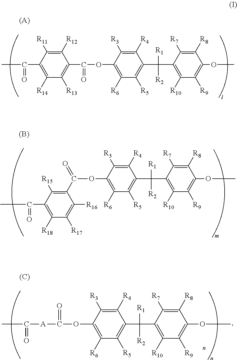
[0054]The example was identical to Manufacturing example 1, except that herein the addition amount of terephthalic acid chloride was 13.346 g, and the addition amount of isophthalic acid chloride was 13.619 g. The polystyrene average molecular weight Mw of the obtained copolymer polyarylate resin (III-2) (23.2 g, yield 48.5%) was 70,200. The structural formula of the copolymer polyarylate resin (III-2) was as follows.

[0055]

[0056]where l:m:n=49:50:1 (molar ratio).

manufacturing example 3

Method for Manufacturing a Copolymer Polyarylate Resin (III-3)

[0057]The example was identical to Manufacturing example 1, except that herein the addition amount of terephthalic acid chloride was 12.802 g, the addition amount of isophthalic acid chloride was 13.619 g, and the addition amount of adipic acid chloride was 0.737 g. The polystyrene average molecular weight Mw of the obtained copolymer polyarylate resin (III-3) (23.5 g, yield 49.2%) was 72,300. The structural formula of the copolymer polyarylate resin (III-3) was as follows.

[0058]

[0059]where l:m:n=47:50:3 (molar ratio).


PUM

PropertyMeasurementUnit
thicknessaaaaaaaaaa
thicknessaaaaaaaaaa
thicknessaaaaaaaaaa

Abstract

Electrophotographic photoconductor including a conductive substrate; and a photosensitive layer provided on the conductive substrate and including at least a charge generation material; a charge transport material; and a resin binder including a copolymer polyarylate resin represented by general formula (I) below:and manufacturing method therefore. Good images with less cracking occurrence are obtained during recycling of a photosensitive drum and peripheral members thereof that includes the electrophotographic photoconductor, and also when a liquid development process is employed.

Description

BACKGROUND OF THE INVENTION[0001]1. Field of the Invention[0002]The present invention relates to an electrophotographic photoconductor (hereafter, also simply referred to as “photoconductor”) and to a manufacturing method thereof, and more particularly to an electrophotographic photoconductor which comprises mainly a conductive substrate and a photosensitive layer containing an organic material, and is used in electrophotographic printers, copiers, fax machines and the like, and to a manufacturing method of the electrophotographic photoconductor.[0003]2. Background of the Related Art[0004]The basic structure of electrophotographic photoconductors comprises a conductive substrate on which there is disposed a photosensitive layer having photoconductive properties. In recent years, organic electrophotographic photoconductors that use organic compounds as functional components for charge generation and charge transport have been the target of active research and development, and have be...

Claims


Application Information

Patent Timeline
Patent Type & Authority Patents(United States)
IPC IPC(8): G03G5/04
CPCG03G5/0564G03G2215/00987G03G2215/00957
Inventor TAKAKI, IKUONAKAMURA, YOICHIKITAGAWA, SEIZONEBASHI, KAZUKIZHU, FENGQIANG
Owner FUJI ELECTRIC CO LTD
Learn More