Material for organic electroluminescence device and organic electroluminescence device

a technology of electroluminescence device and material, which is applied in the direction of thermoelectric devices, discharge tube luminescnet screens, natural mineral layered products, etc., can solve the problems of low luminous efficiency and achieve the effects of reducing durability, low luminous efficiency and improving luminous efficiency

Active Publication Date: 2013-04-09
UDC IRELAND
View PDF22 Cites 4 Cited by
  • Summary
  • Abstract
  • Description
  • Claims
  • Application Information

AI Technical Summary

Benefits of technology

[0068]When the content of the fluorine atom of the phosphorescent metal complex is less than 7% by mass, the minimum triplet energy and the energy in a highly excited state are not sufficiently separated from each other, and the transition into a highly excited state still possibly takes place, and therefore, an effect of the invention, i.e., an enhancement of the luminous efficiency, is not proved.
[0069]Also, the phosphorescent metal complexes disclosed in US-A-2008 / 297033 and JP-A-2008-311607 have a ligand with a large surface area and have a structure where the ligand is three-dimensionally spread by an octahedral 6-coordinate structure. For that reason, the packing state among molecules does not become close but is in a state where a number of voids are present, and a chemical potential of the solid state is not stabilized so much. Therefore, it may be supposed that melting takes place in vacuo at the time of sublimation purification, thereby reducing a sublimation rate. It may be considered that when a fluorine atom is introduced into the ligand as in the invention, packing in the solid state is improved by an effect of fluorine having a strong electronegativity for attracting an electron cloud, and mutual stabilization of molecules in a solution state is inhibited due to a reduction in an intermolecular interaction to increase the chemical potential, thereby obtaining an improving effect of the sublimation purification time.
[0070]Also, there is a close relation between a crystal form and a sublimation temperature, and it may be guessed that the fact that by introducing a fluorine atom, the crystal form of a coarse body is changed is also one of the factors.
[0071]In the thus obtained material, a voltage increase to be caused following driving when formed into a device is small. It may be estimated that this is caused due to the fact that since the time when it is exposed to a high temperature at the time of sublimation purification is short, the kind of impurities to be contained is different as compared with usual materials. Though various causes for which the voltage increases at the time of device driving may be considered, charge transporting properties of the material having been decomposed within the light emitting layer are poor, and therefore, it may be considered that a flow of both charges is disturbed. A possibility that infinitesimal impurities promote the decomposition within the luminescence device has already been suggested, and it may be supposed that this decomposition route was altered by changing the purification method.
[0072]When the content of the fluorine atom of the specified phosphorescent metal complex is excessively high, the improving effect of the sublimation purification time becomes inversely small, and the complex is coagulated in the device prepared using the obtained material so that the hue is deteriorated, too. For those reasons, the content of the fluorine atom of the specified phosphorescent metal complex is preferably 7% by mass or more and not more than 50% by mass, and more preferably 10% by mass or more and not more than 35% by mass.
[0073]In the invention, though the specified phosphorescent metal complex has a content of the fluorine atom of 7% by mass or more, it may be one containing a fluorine atom only in the main ligand, may be one containing a fluorine atom only in the ancillary ligand, or may be one containing a fluorine atom in both the main ligand and the ancillary ligand. The metal complex containing a fluorine atom in the main ligand is preferable because the effect of the invention is highly obtainable. Also, the metal complex containing a fluorine atom only in the ancillary ligand is preferable in view of the fact that the synthesis is easy as compared with the metal complex containing a fluorine atom in the main ligand. In this respect, the phosphorescent metal complex in the invention has a bidentate ligand represented by the formula (A1-1) or (A3-1) as a main ligand.

Problems solved by technology

However, organic EL devices using an iridium complex disclosed in US-A-2008 / 297033 and JP-A-2008-311607 involve such a problem that the luminous efficiency is low.
Also, there is involved such a problem that light emission obtained from such an organic EL device is long in a wavelength so that the light emission does not become purely blue.

Method used


Image

  • Material for organic electroluminescence device and organic electroluminescence device
  • Material for organic electroluminescence device and organic electroluminescence device
  • Material for organic electroluminescence device and organic electroluminescence device

Examples


example 1

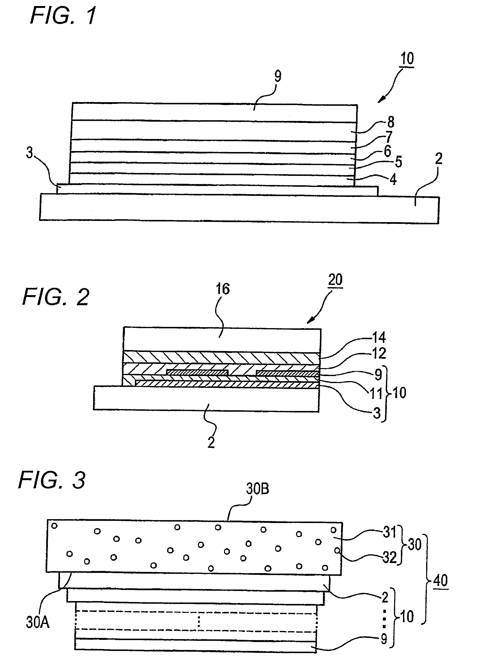
[0322]An indium tin oxide (ITO) film-provided glass substrate having a thickness of 100 μm and a size of 2.5 cm in square (manufactured by Geomatec Co., Ltd., surface resistance: 10Ω / □) was put in a washing vessel, ultrasonically washed in 2-propanol and then subjected to a UV-ozone treatment for 30 minutes. The following organic layers were successively vapor deposited on this transparent anode (ITO film) by means of vacuum vapor deposition.

[0323]First layer: CuPc (copper phthalocyanine), film thickness: 120 nm

[0324]Second layer: NPD (N,N′-di-α-naphthyl-N,N′-diphenyl)-benzidine), film thickness: 7 nm

[0325]Third layer: CBP (4,4′-di(9-carbazoyl)biphenyl), film thickness: 3 nm

[0326]Fourth layer (light emitting layer): Dopant (9% by mass), host material (91% by mass), film thickness: 30 nm

[0327]Fifth layer: First electron transport material (BAlq), film thickness: 30 nm

[0328]1 nm-thick lithium fluoride and 100 nm-thick metallic aluminum were vapor deposited in this order thereon, there...

example 2

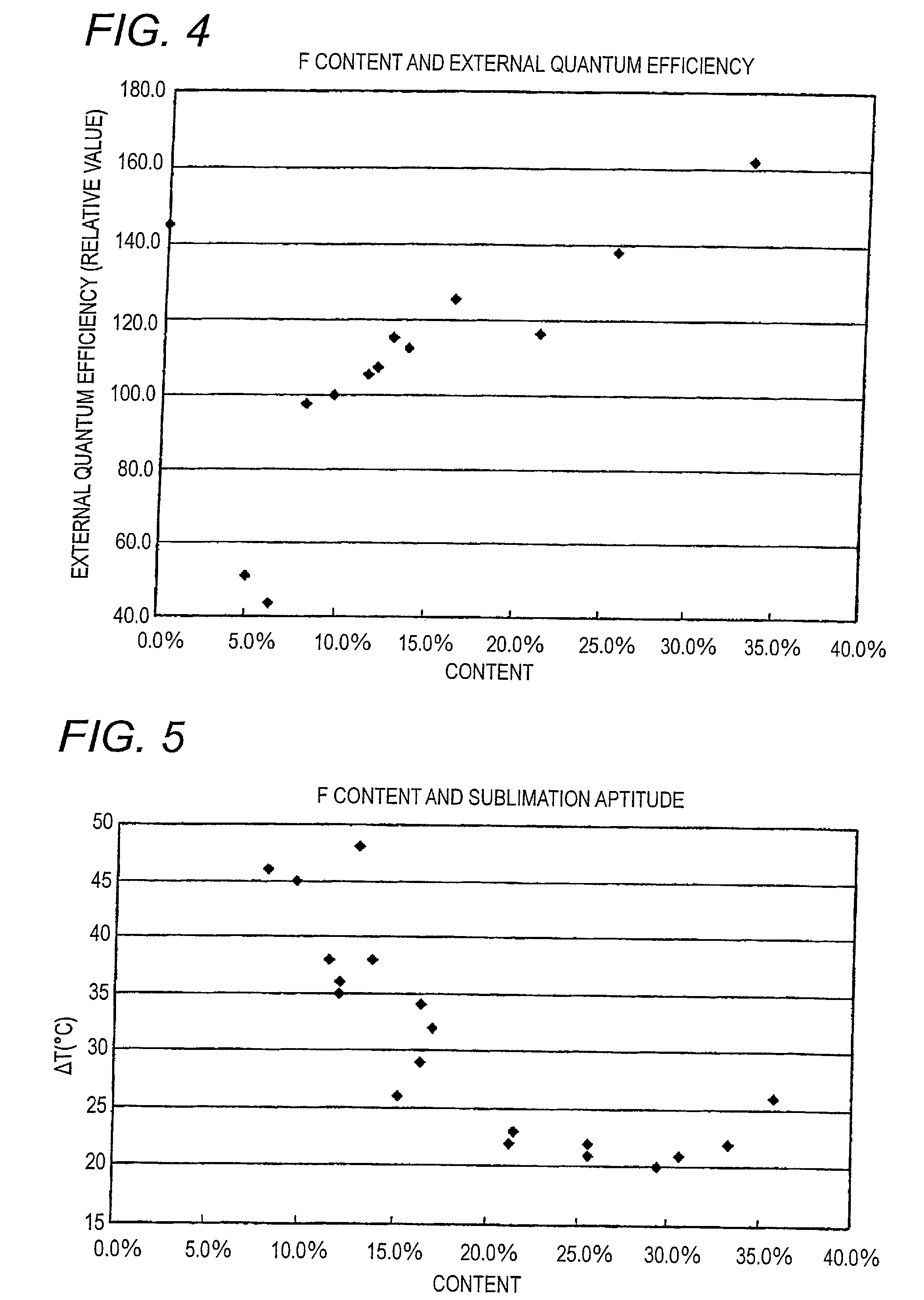
[0337]With respect to each of the compounds of the invention and the comparative compounds, a TG curve at 1×10⁻² Pa was measured in a sample amount of 20 mg, and a temperature (T(−5%)) at a [(weight loss percent)−5%] point (since all of purities of the samples are 97% or more in terms of an HPLC area ratio, the −5% point was regarded as a temperature at which sublimation and evaporation were started) and a temperature (T(end)) at a point where the weight loss was completed were measured. In this respect, all of the measurements are carried out while elevating the temperature at a rate of 1° C. per minute. Also, sublimation purification was carried out at the temperature T(end) in a starting weight of 500 mg under the same pressure, and a purification yield thereof was evaluated. Also, a graph plotting a relation between a fluorine atom content and a sublimation aptitude (ΔT) is shown in FIG. 5.

[0338]Next, a device having the following constitution was prepared using the obtained mat...

example 3

[0349]An indium tin oxide (ITO) film-provided glass substrate having a thickness of 100 μm and a size of 2.5 cm in square (manufactured by Geomatec Co., Ltd., surface resistance: 10Ω / □) was put in a washing vessel, ultrasonically washed in 2-propanol and then subjected to a UV-ozone treatment for 30 minutes. The following organic layers were successively vapor deposited on this transparent anode (ITO film) by means of vacuum vapor deposition.

[0350]First layer: CuPc (copper phthalocyanine), film thickness: 120 nm

[0351]Second layer: NPD (N,N′-di-α-naphthyl-N,N′-diphenyl)-benzidine), film thickness: 7 nm

[0352]Third layer: Charge transport material, film thickness: 2 nm

[0353]Fourth layer (light emitting layer): Dopant (12% by mass), host material (88% by mass), film thickness: 30 nm

[0354]Fifth layer: First electron transport material (BAlq), film thickness: 30 nm

[0355]1 nm-thick lithium fluoride and 100 nm-thick metallic aluminum were vapor deposited in this order thereon, thereby formi...


PUM

PropertyMeasurementUnit
thicknessaaaaaaaaaa
thicknessaaaaaaaaaa
thicknessaaaaaaaaaa

Abstract

A material for an organic electroluminescence device including a phosphorescent metal complex containing a monoanionic bidentate ligand represented by the following formula (A1-1) or formula (A3-1) as defined in the specification and a non-radiative metal having an atomic weight of 40 or more, an organic electroluminescence device including the material for an organic electroluminescence device, and a light emitting unit, a display unit and an illumination unit each including the organic electroluminescence device are provided.

Description

TECHNICAL FIELD[0001]The present invention relates to a material for organic electroluminescence device and an organic electroluminescence device.BACKGROUND ART[0002]In recent years, in view of the fact that light emission with a high brightness is obtainable through low-voltage driving, an organic electroluminescence device (hereinafter also referred to as “device” or “organic EL device”) has been actively researched and developed. In general, the organic electroluminescence device is constituted of an organic layer including a light emitting layer and a pair of electrodes interposing this light emitting layer therebetween, and energy of an exciton generated through recombination of an electron injected from a cathode and a hole injected from an anode is utilized for the light emission.[0003]In recent years, an improvement of efficiency of the device is being advanced by using a phosphorescent material. For example, an organic electroluminescence device having enhanced luminous eff...

Claims


Application Information

Patent Timeline
Patent Type & Authority Patents(United States)
IPC IPC(8): H01L51/54C09K11/06
CPCC07F15/0033C09K11/06H01L51/0052H01L51/0067H01L51/0085H01L51/5016H05B33/14C09K2211/1044C09K2211/1051C09K2211/185H10K85/615H10K85/654H10K85/342H10K50/11H10K2101/10H10K85/00
Inventor TAKADA, SAKI
Owner UDC IRELAND
Why Eureka
Try Eureka