Method for the production of multiplayer electrostatic lens array

a technology of electrostatic lens array and multi-layer technology, which is applied in the direction of mass spectrometer, particle separator tube, instruments, etc., can solve the problems of difficult phase plate phase plate realization, difficult photosensitive samples, and often only being loaded, etc., to achieve the effect of being versatile and improving

Inactive Publication Date: 2013-07-16
GERTHSEN DAGMAR +2
View PDF11 Cites 6 Cited by
  • Summary
  • Abstract
  • Description
  • Claims
  • Application Information

AI Technical Summary

Benefits of technology

[0023]A further object of the invention is to provide a versatile and improved method for the production of microlenses or nanolenses in general.
[0024]Yet another object of the invention is to provide a simple, cost-effective method for the production of a microlens or nanolens arrangement that is suitable for serial production, in particular of a Boersch phase plate with high yield.
[0025]Still another object of the invention is to provide a well manageable, stable, qualitatively high-value and cost-effective microlens and nanolens arrangement or Boersch phase plate.
[0039]The through hole through the five layers is preferably carried out by means of micromilling or nanomilling. For this purpose in special measure a device with which a focused ion beam can be produced and controlled (so-called focused-ion-beam device” or “Fokussierter-Ionenstrahl-Gerät”) is suitable. By means of the focused ion beam the layer material is sputtered off locally, so that the borehole is cut out. This method facilitates in advantageous manner a very precise incision and avoids short circuits between the layers. The minimum achievable diameter of the hole depends on the diameter of the ion beam and the thickness of the layer arrangement. Further along with circular geometries also other lens forms like e.g. quadrupole-octupole or hexapole symmetries can be produced.
[0041]The production of the lens in the case of a chip with a membrane window is preferably concluded with the production of the hole. In the case of the usage of multi-membrane wafers subsequently the wafers can be divided up into individual chips with preferably one or more membrane window(s) each. It is advantageous, in particular in a TEM to use a chip with several, if necessary even different lens arrangements or phase plates, since these can then be replaced in advantageous manner without breaking the vacuum. Also a chip can contain additional free windows.

Problems solved by technology

This is very awkward and tedious.
Further complicating matters in the recording of image series is the fact that the samples are frequently photosensitive and can only be loaded with a low electron dose without significant radiation damage.
However, the technical realization of a phase plate for a TEM is extraordinarily difficult, a fact which lies in the extremely small wavelength of the electrons in the magnitude of 10−12 m in comparison to the wavelength of visible light (4 . . . 7×10⁻⁷ m).
The usage of such a Zernicke phase plate has proved impracticable up to now due to the following difficulties.
Further the granularity of the carbon film leads to spatial fluctuations of the phase displacement.
In addition the carbon film is damaged by the high-energy electrons.
The spatial inhomogeneous contamination of the carbon film connected to the slight thickness of about 3×10⁻⁸ leads to electrical charges and uncontrollable phase displacements.
If said thickness changes, for example through contamination, the plate must be expensively removed and replaced by a new plate.
In principle, setting of the phase displacement is not possible without replacement of the plate.
The proposed structure however is expensive and extremely cost-intensive.
The extraordinary difficulty lies in the small dimension of the phase plate and its nevertheless complex structure.
However, the method is complicated by a multitude of depositing and etching steps as well as the removal of the auxiliary substrate.
In addition a great probability exists that in the event of the removal of the auxiliary substrate the highly sensitive phase plate will be destroyed.

Method used


Image

  • Method for the production of multiplayer electrostatic lens array
  • Method for the production of multiplayer electrostatic lens array
  • Method for the production of multiplayer electrostatic lens array

Examples


Embodiment Construction

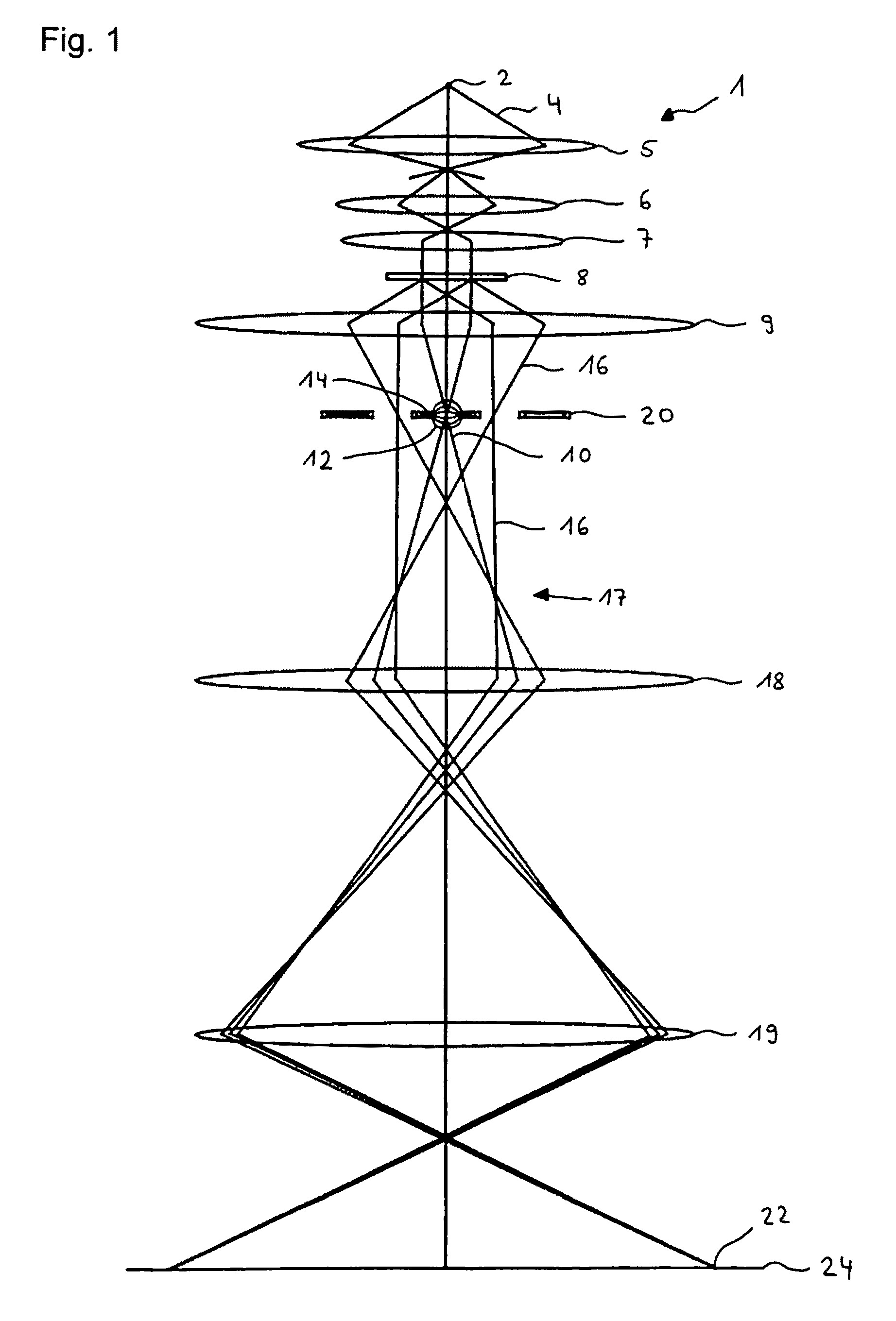
[0079]FIG. 1 shows a transmission electron microscope 1 with a phase plate 20, as described in the introduction.

[0080]A plane base for the building of a layer arrangement is important for the practicability of later structuring steps in the course of the present invention. Said base can be metallic or insulating. The thickness of the base decisively influences the entire thickness of the lens arrangement to be produced. Within the framework of the invention therefore very thin membranes are used as base. The membrane becomes a component of the lens arrangement to be produced. Herewith the overall thicknesses of the lens arrangement of less than 100 nm can be realized.

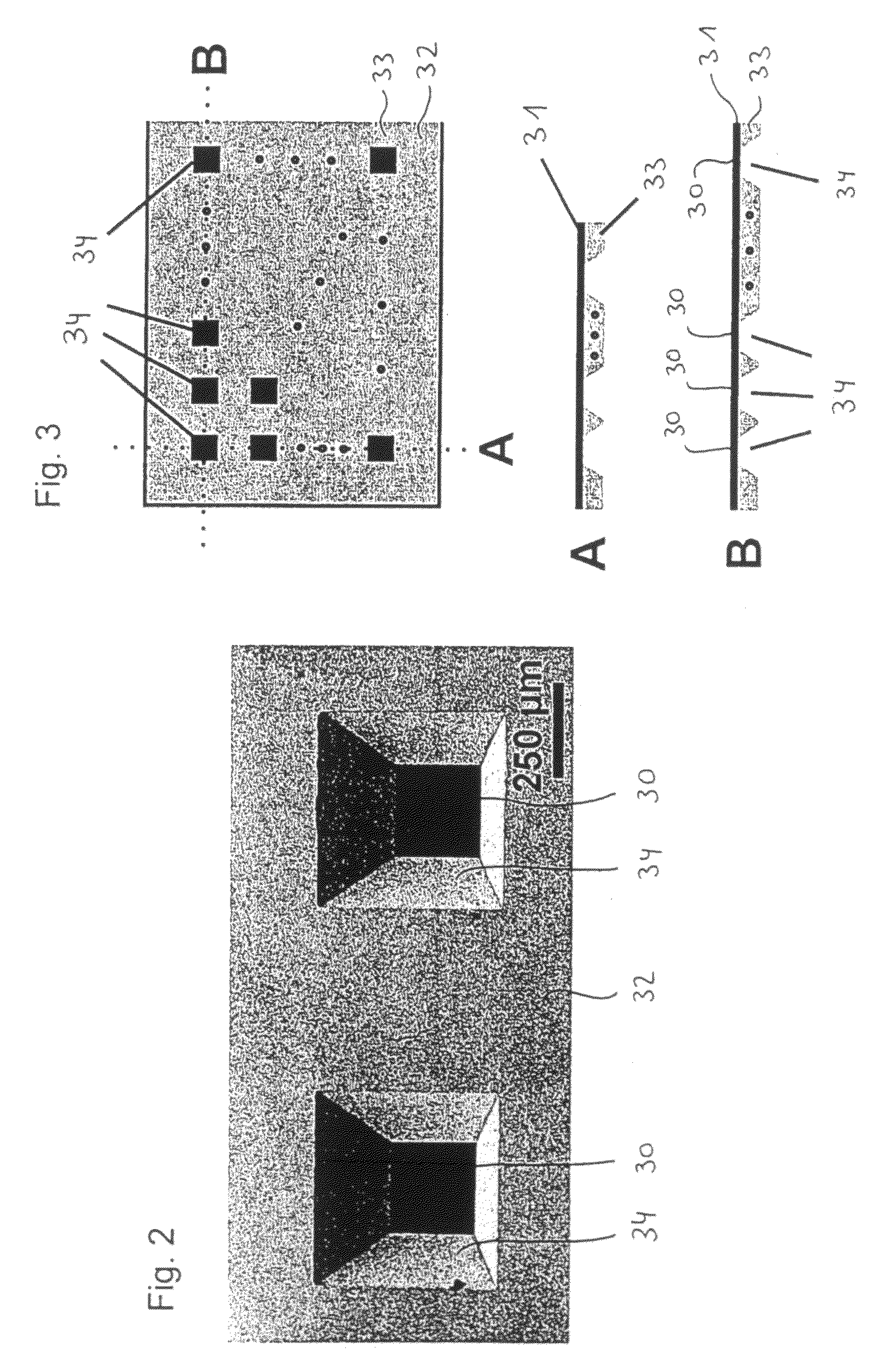
[0081]With reference to FIG. 2 a silicon enriched silicon nitride layer about 100 nm thin deposited on a silicon wafer is used, said layer forming a self-supporting silicon nitride membrane 30 in each of two membrane windows 34. Said membrane has proven to be particularly suitable, in particular since silicon nitride is...


PUM

PropertyMeasurementUnit
diameteraaaaaaaaaa
diameteraaaaaaaaaa
thicknessaaaaaaaaaa

Abstract

The invention relates to a method for the production of a multilayer electrostatic lens arrangement with at least one lens electrode in general, a method for the production of a phase plate in particular as well as the lens arrangement, the phase plate and a transmission electron microscope with the phase plate.The lens arrangement or the phase plate is produced from a thin self-supporting silicon nitride membrane which is fixed in a macroscopic chip with deposition of further layers.The central bore as well as the aperture opening are milled out by means of an ion beam.

Description

FIELD OF THE INVENTION[0001]The invention relates to a method for the production of a multi-layer electrostatic lens arrangement with at least one lens electrode in general, a method for the production of a phase plate in particular as well as the lens arrangement, the phase plate and a transmission electron microscope with the phase plate.BACKGROUND OF THE INVENTION[0002]The present invention arose from the need to produce a so-called Boersch phase plate. However, the method developed by the inventors can also be used for the production of other multi-layer electrostatic lens arrangements.[0003]One frequently employed method for the examination of the structure of for example biological-medical objects is transmission electron microscopy (TEM), with which a resolution in the range of less than 1 nm can be achieved. With this, structural details of an object in the range of nearly atomic dimensions can be depicted. Biological objects consist however predominantly of light elements l...

Claims


Application Information

Patent Timeline
Patent Type & Authority Patents(United States)
IPC IPC(8): G21K5/04H01J37/24
CPCH01J37/12H01J37/26H01J37/263Y10T29/49117H01J2237/2614H01J2237/31749H01J2237/226
Inventor GERTHSEN, DAGMARPEREZ-WILLARD, FABIANSCHULTHEISS, KATRIN
Owner GERTHSEN DAGMAR
Why Eureka
Try Eureka