Power light emitting diode and method with current density operation

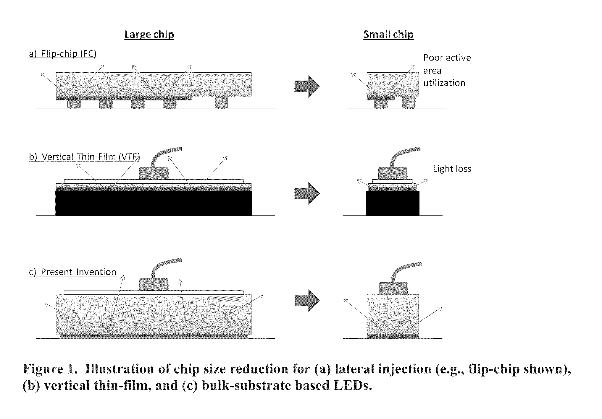
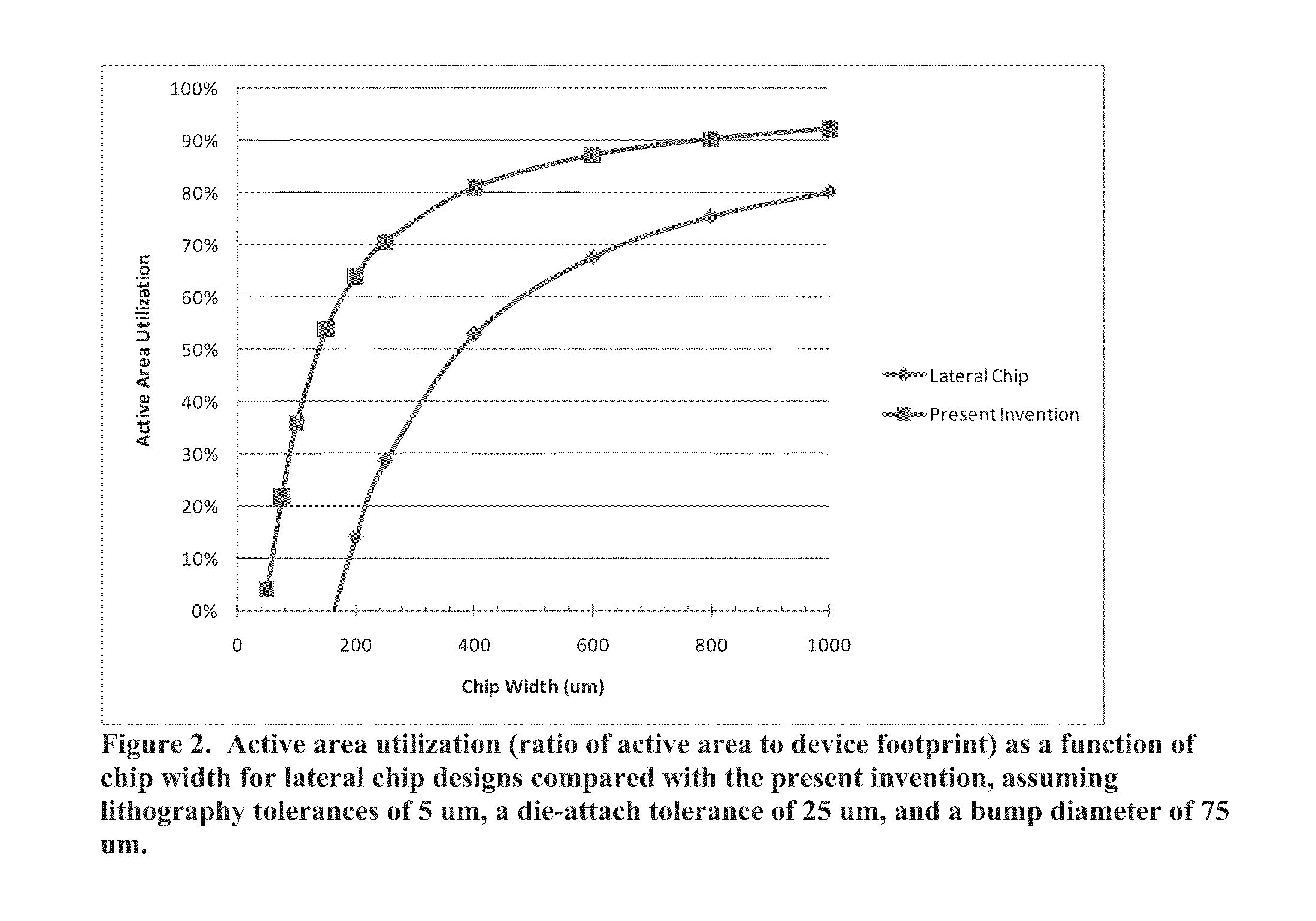
a power light emitting diode and current density technology, applied in the direction of electric variable regulation, process and machine control, instruments, etc., can solve the problems of reducing active area utilization, reducing the size of lateral chips, and practical limit on die size, so as to reduce the area required for led semiconductors, reduce cost, and high light extraction efficiency

Active Publication Date: 2013-08-06
KORRUS INC
View PDF166 Cites 45 Cited by
  • Summary
  • Abstract
  • Description
  • Claims
  • Application Information

AI Technical Summary

Benefits of technology

[0010]For a fixed light output level, the main lever for reducing cost is by decreasing the LED semiconductor area required for the lighting product. Reducing the total LED chip area effectively increases semiconductor manufacturing plant output, while reducing the size of optics and other components used in final product assembly. Reducing chip size increases current density, but high external quantum efficiency may be maintained at high current density using epitaxial techniques of the present invention described below. Chip design also plays a critical role. Chip size reduction for lateral chips (either top or substrate emitting) is problematic as fabrication tolerances can reduce active area utilization as chip size is reduced.
[0011]This effect is illustrated in FIG. 1. Lateral-injection devices (whether top or bottom contacted) require area for making both anode and cathode connections on the same side of the device. This fundamentally reduces active area utilization (portions of the die footprint are required for the cathode) and puts a practical limit on die size. Assuming lithography tolerances of 5 um, a die-attach tolerance of 25 um, and a bump diameter of 75 um, the active area utilization vs. chip width is as shown in the Figure. For SiC, a conductive buffer layer approach allows the use of a vertical injection design. However, the lattice mismatch between SiC and GaN results in high dislocation densities (>1×108 cm-2) which can cause unreliability at high power densities. Also, SiC has a higher refractive index than GaN, making the issue of light extraction a more difficult problem.
[0023]The device and method herein provide for higher yields over conventional techniques in fabricating LEDs. In other embodiments, the present method and resulting structure are easier to form using conventional techniques and gallium and nitrogen containing substrate materials having polar, non-polar or semipolar surface orientations. The present invention provides a resulting device and method for high current density LED devices having smaller feature sizes and substantially no “Droop.” In a preferred embodiment, the device provides a resulting white light fixture that uses substantially reduced LED semiconductor area, as compared to conventional devices. In a preferred embodiment, the present LED active region designs are configured for reducing droop, enabling chip architectures that operate efficiently at high current densities.

Problems solved by technology

Chip size reduction for lateral chips (either top or substrate emitting) is problematic as fabrication tolerances can reduce active area utilization as chip size is reduced.
This fundamentally reduces active area utilization (portions of the die footprint are required for the cathode) and puts a practical limit on die size.
However, the lattice mismatch between SiC and GaN results in high dislocation densities (>1×108 cm-2) which can cause unreliability at high power densities.
Also, SiC has a higher refractive index than GaN, making the issue of light extraction a more difficult problem.

Method used


Image

  • Power light emitting diode and method with current density operation
  • Power light emitting diode and method with current density operation
  • Power light emitting diode and method with current density operation

Examples


Embodiment Construction

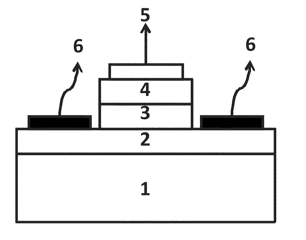
[0038]This invention relates generally to lighting techniques, and in particular to techniques for high current density LED devices fabricated on bulk gallium and nitrogen containing polar, semipolar or nonpolar materials. The invention can be applied to applications such as white lighting, multi-colored lighting, lighting for flat panel displays, other optoelectronic devices, and similar products.

[0039]We have discovered that recent breakthroughs in the field of GaN-based optoelectronics have demonstrated the great potential of devices fabricated on bulk polar, nonpolar and semipolar GaN substrates. Specifically for nonpolar and semipolar orientations, the lack of strong polarization induced electric fields that plague conventional devices on c-plane GaN leads to a greatly enhanced radiative recombination efficiency in the light emitting InGaN layers. For polar materials, the deleterious effects of polarization fields may be reduced by reducing the InN content of the active region,...


PUM


Abstract

A light emitting diode device emitting at a wavelength of 390-415 nm has a bulk gallium and nitrogen containing substrate with an active region. The device has a current density of greater than about 175 Amps / cm2 and an external quantum efficiency with a roll off of less than about 5% absolute efficiency.

Description

CROSS-REFERENCE TO RELATED APPLICATION[0001]This application claims priority to U.S. Ser. No. 61 / 243,988, filed Sep. 18, 2009, commonly assigned, and hereby incorporated by reference herein.BACKGROUND OF THE INVENTION[0002]This invention relates generally to lighting techniques, and in particular to techniques for high current density LED devices fabricated on bulk gallium and nitrogen containing polar, semipolar or nonpolar materials. The invention can be applied to applications such as white lighting, multi-colored lighting, lighting for flat panel displays, other optoelectronic devices, and similar products.[0003]In the late 1800's, Thomas Edison invented the light bulb. The conventional light bulb, commonly called the “Edison bulb,” has been used for over one hundred years. The conventional light bulb uses a tungsten filament enclosed in a glass bulb sealed in a base, which is screwed into a socket. The socket is coupled to AC power or DC power. The conventional light bulb can b...

Claims


Application Information

Patent Timeline
Patent Type & Authority Patents(United States)
IPC IPC(8): H05B37/02H01L29/22
CPCH05B37/02H01L33/405H01L33/32H01L33/16H01L2224/16H01L2224/48H05B47/10H01L33/04
Inventor KATONA, THOMAS M.RARING, JAMES W.D'EVELYN, MARK P.KRAMES, MICHAEL R.
Owner KORRUS INC
Why Eureka
Try Eureka