Field-effect transistor, and process for producing field-effect transistor

a field-effect transistor and field-effect technology, applied in the direction of semiconductor/solid-state device manufacturing, semiconductor devices, electrical equipment, etc., can solve the problems of high energy cost, difficult film formation directly on a large-sized glass substrate, and inability to meet the requirements of high-efficiency semiconductor devices, etc., to achieve the effect of reducing the degree of freedom of the production process and facilitating the production of semiconductor devices

Active Publication Date: 2013-09-10
IDEMITSU KOSAN CO LTD
View PDF10 Cites 27 Cited by
  • Summary
  • Abstract
  • Description
  • Claims
  • Application Information

AI Technical Summary

Benefits of technology

[0018]Further, due to the amorphous nature, an amorphous transparent semiconductor thin film has a poor resistance to chemicals such as an etching solution, the representative example of which is PAN, and hence, it has disadvantages that wet etching of a metal wiring on a semiconductor film cannot be conducted, a refractive index is too large to allow the transmittance of a multilayer film to deteriorate easily. Moreover, due to the amorphous nature, the film adsorbs oxygen, water or the like in an atmospheric gas, and hence, the electric characteristics thereof may change, resulting in a lowered yield.
[0094]Due to the PAN resistance, the degree of freedom of the production process is increased, whereby the semiconductor device can be produced efficiently.

Problems solved by technology

A transistor using the above-mentioned silicon thin film is produced by using a silane-based gas, and hence, it is disadvantageous in respect of safety or equipment cost.
In addition, since an amorphous silicon thin film has a small band gap, it may absorb visible rays to cause malfunction.
Moreover, a polycrystalline silicon thin film requires a heating process which is conducted at relatively high temperatures, thereby incurring a large amount of energy cost.
In addition, this film is hard to be formed directly on a large-sized glass substrate.

Method used


Image

  • Field-effect transistor, and process for producing field-effect transistor
  • Field-effect transistor, and process for producing field-effect transistor
  • Field-effect transistor, and process for producing field-effect transistor

Examples


first application example

OF SELF-ALIGNMENT

[0136]Next, the first and second application examples of the self-alignment will be explained with reference to the drawing.

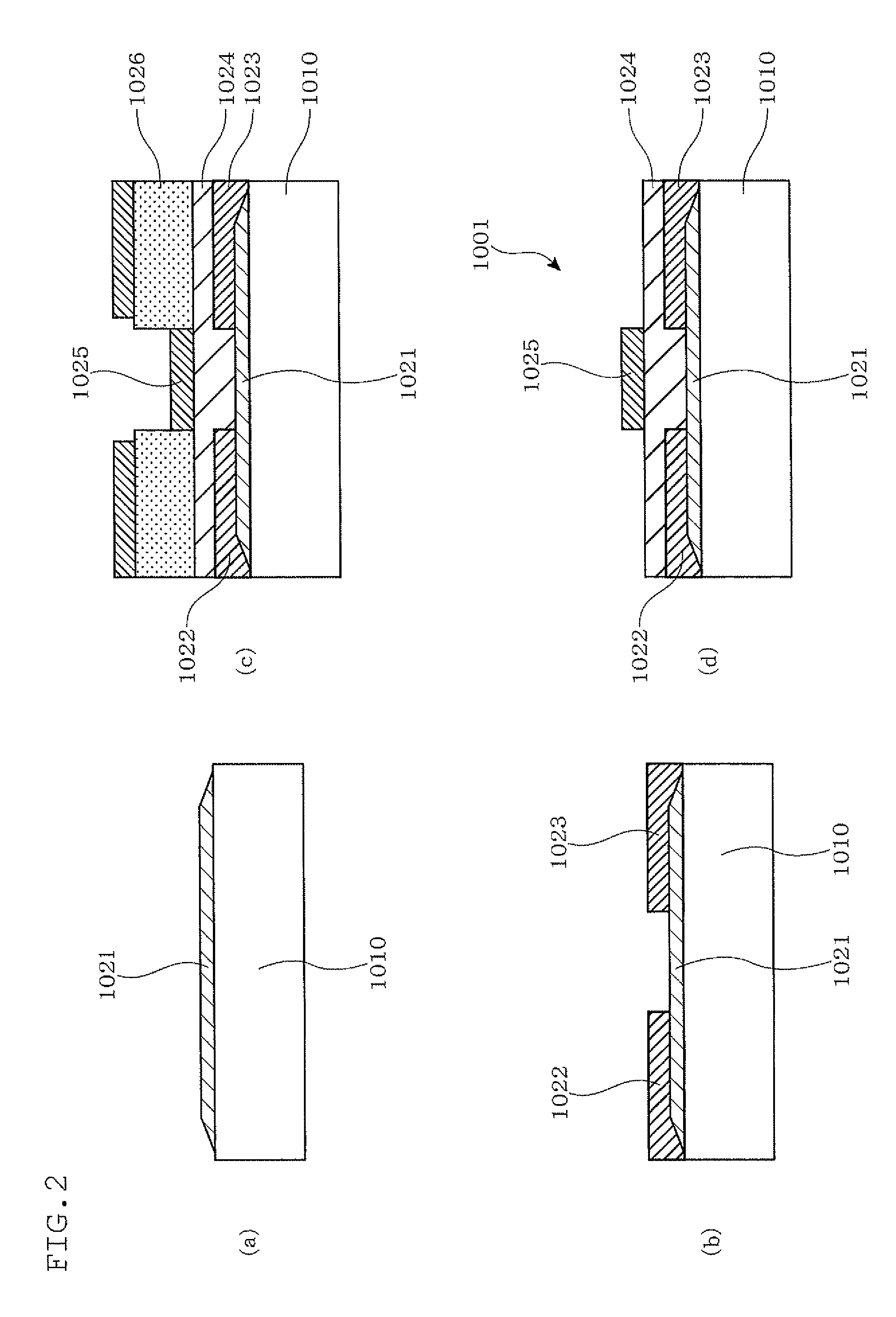
[0137]FIG. 3 is a schematic view, for explaining self-alignment, of essential parts of a first application example of a field-effect thin film transistor according to one embodiment of the present invention, in which (a) is a cross-sectional view showing the state in which a crystalline oxide is formed, (b) is a cross-sectional view showing the state in which a source electrode and a drain electrode are formed, (c) is a cross-sectional view showing the state in which a gate-insulating film, a resist and a gate electrode are stacked, and (d) is a cross-sectional view showing the state in which the gate electrode is formed.

[0138]First, as shown in FIG. 3(a), in a top-gate type field-effect thin film transistor 1001a, a Mo / Al / Mo film and an IZO film (using a target containing 10.7 wt % of zinc oxide and 89.3 wt % of indium oxide) are formed on a t...

second application example

OF SELF-ALIGNMENT

[0145]FIG. 4 is a schematic view, for explaining self-alignment, of essential parts of a second application example of a field-effect thin film transistor according to one embodiment of the present invention, in which (a) is a cross-sectional view showing the state in which a gate electrode is formed, (b) is a cross-sectional view showing the state in which the gate-insulating film is stacked and a crystalline oxide is formed, (c) is a cross-sectional view showing the state in which a resist, a source electrode and a drain electrode are stacked, and (d) is a cross-sectional view showing the state in which the source electrode and the drain electrode are formed.

[0146]First, as shown in FIG. 4(a), in the bottom-gate type field-effect thin film transistor 1001b, the gate electrode 1025 formed of a metal thin film is formed on the transparent glass substrate 1010.

[0147]Next, as shown in FIG. 4(b), on the glass substrate 1010 and the gate electrode 1025, the gate-insulat...

example 1

FILM-FORMING EXAMPLE 1

(First Film-forming Method: Sputtering Method)

[0191]In this film formation method, it is preferable to use the vapor phase deposition method which uses, as a target, an indium oxide polycrystalline sintered body with a composition of In2O3(ZnO)m (wherein m is an integer of 2 to 20). Of the vapor deposition methods, the sputtering method and the pulse laser deposition method are suitable. The sputtering method is most suitable in view of mass productivity.

[0192]However, if the amorphous film is formed under normal conditions, oxygen deficiency mainly occurs. Therefore, it has been impossible to allow the electron carrier concentration to be less than 1018 / cm3, which means an electrical resistance of 102 Ωcm or more. If such a film is used, a normally-off transistor cannot be configured.

[0193]Therefore, the inventors prepared an amorphous zinc oxide-containing indium oxide by the sputtering method using the sputtering apparatus shown in FIG. 5. Then, the indium o...


PUM


Abstract

To provide a field-effect transistor improved in transparency, electrical properties, stability, uniformity, reproducibility, heat resistance and durability, and as a reduced overlap capacity between electrodes.A field-effect thin film transistor 1001 includes a gate electrode 1025, an active layer, a source electrode 1022 and a drain electrode 1023, wherein a crystalline oxide 1021 containing indium and having an electron carrier concentration of less than 1018 / cm3 is used as the active layer, and the gate electrode 1025 is in self-alignment with the source electrode 1022 and the drain electrode 1023. The crystalline oxide 1021 contains a positive trivalent element different from a positive divalent element or indium.

Description

TECHNICAL FIELD[0001]The present invention relates to a field-effect transistor and a method for producing a field-effect transistor. In this field-effect transistor, a crystalline oxide with a predetermined electron carrier concentration is used as an active layer, and a gate electrode is in self-alignment with a source electrode and a drain electrode. In the method for producing a field-effect transistor, a crystalline oxide with a prescribed electron carrier concentration is used as an active layer.BACKGROUND ART[0002]An active-matrix type display apparatus such as an LCD (liquid crystal display) and an organic EL (Electro Luminescence) display apparatus is widely used in respect of display performance, energy saving, or the like. In particular, the active-matrix type display apparatus has almost come to constitute the mainstream of a display for cellular phones, PDAs (personal digital assistance), PCs, lap-top PCs, TVs or the like. In these display apparatuses, a TFT (field-effe...

Claims


Application Information

Patent Timeline
Patent Type & Authority Patents(United States)
IPC IPC(8): H01L29/12H01L31/072H01L31/109
CPCH01L29/66969H01L29/7869
Inventor INOUE, KAZUYOSHIYANO, KOKIKASAMI, MASASHI
Owner IDEMITSU KOSAN CO LTD
Why Eureka
Try Eureka