Method of plasma preparation of metallic contacts to enhance mechanical and electrical integrity of subsequent interconnect bonds

a technology of interconnection bonding and metallic contact, which is applied in the field of surface preparation of metallic contact, can solve the problems of chemical and its subsequent disposal cost, reliability problems, and liquid-borne or airborne contamination of devices, and achieve the effects of not damage sensitive electronic circuits or components, inhibiting further oxidation, and quick drying

Active Publication Date: 2013-10-29
ONTOS EQUIP SYST
View PDF12 Cites 7 Cited by
  • Summary
  • Abstract
  • Description
  • Claims
  • Application Information

AI Technical Summary

Problems solved by technology

Example drawbacks of acid chemical etching include the potential for liquid-borne or airborne contamination of the devices, handling damage to delicate chips, a residue of acid etchant on the surface of the components which can lead to reliability problems, cost of chemicals and their subsequent disposal, a slow process turnaround time, usage of toxic and dangerous chemicals, the need for corrosion-resistant etching hardware and enclosures, high maintenance requirements, the need for toxic / corrosive exhaust provisions, and unwanted chemical reactions between the etchant and other surface features of the chips.
Example drawbacks of vacuum plasma etching for oxide removal include expensive vacuum plasma equipment, slow process turnaround time, potential for plasma damage to the components by hot electrons, ions, and high kinetic energy atoms, back-sputtering of unwanted metals from vacuum chamber components or from the substrate itself onto the substrate being cleaned, expensive and time-consuming maintenance requirements of the required equipment, and a higher level of operator proficiency and training needed to run sophisticated vacuum plasma systems.
Additionally, and very significantly, these methods only very temporarily remove oxidation from the metallic contacts, since the oxide regrows rapidly when exposed to air after the oxide reduction process.
This poses two problems: 1) equipment and process time required to remove the oxidation inhibiting layer are costly and time-consuming; and 2) once the oxidation inhibiting layer is removed, the surface is once again subject to re-oxidation prior to the bonding.
These chambers impose additional time, expense, bulk, and complexity to the bonding process and equipment.

Method used


Image

  • Method of plasma preparation of metallic contacts to enhance mechanical and electrical integrity of subsequent interconnect bonds
  • Method of plasma preparation of metallic contacts to enhance mechanical and electrical integrity of subsequent interconnect bonds
  • Method of plasma preparation of metallic contacts to enhance mechanical and electrical integrity of subsequent interconnect bonds

Examples


Embodiment Construction

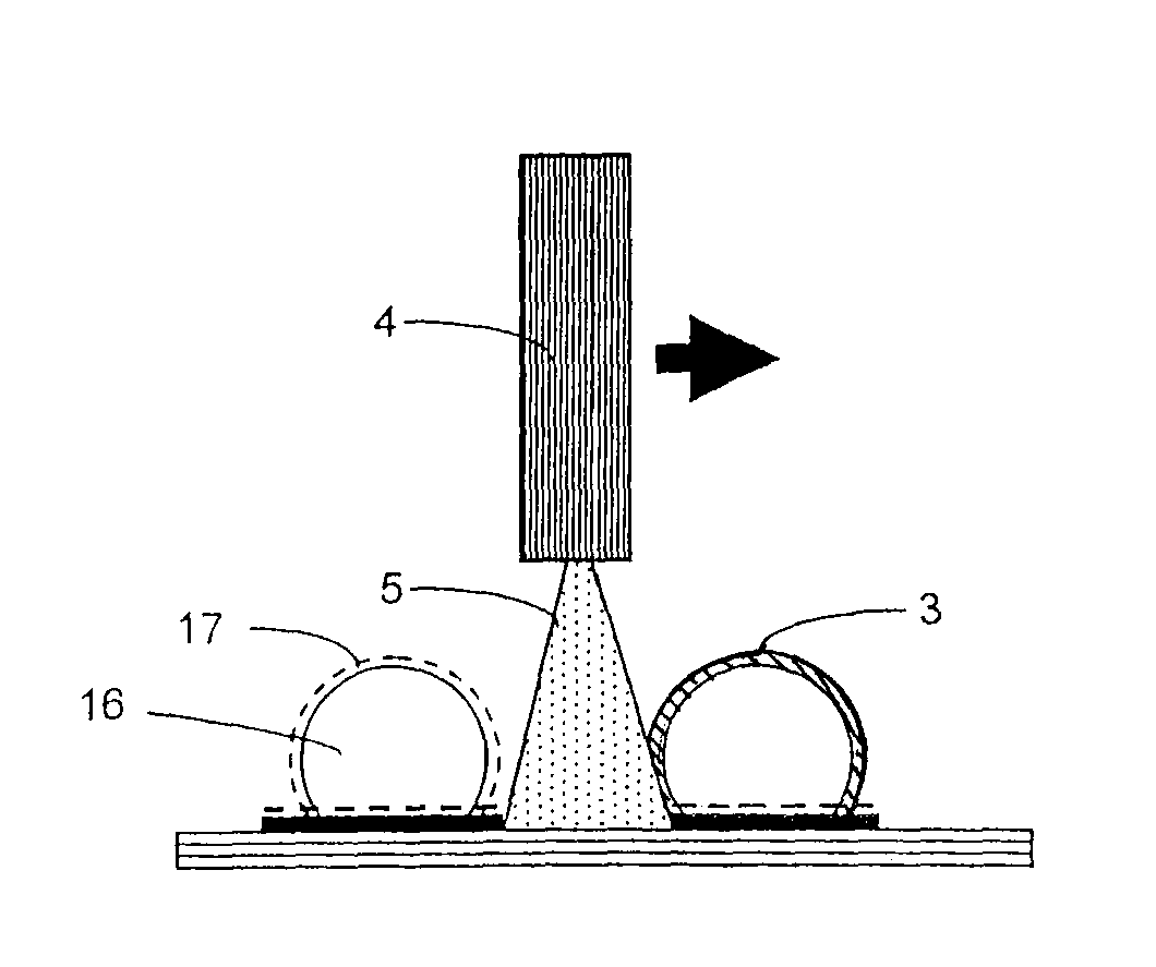
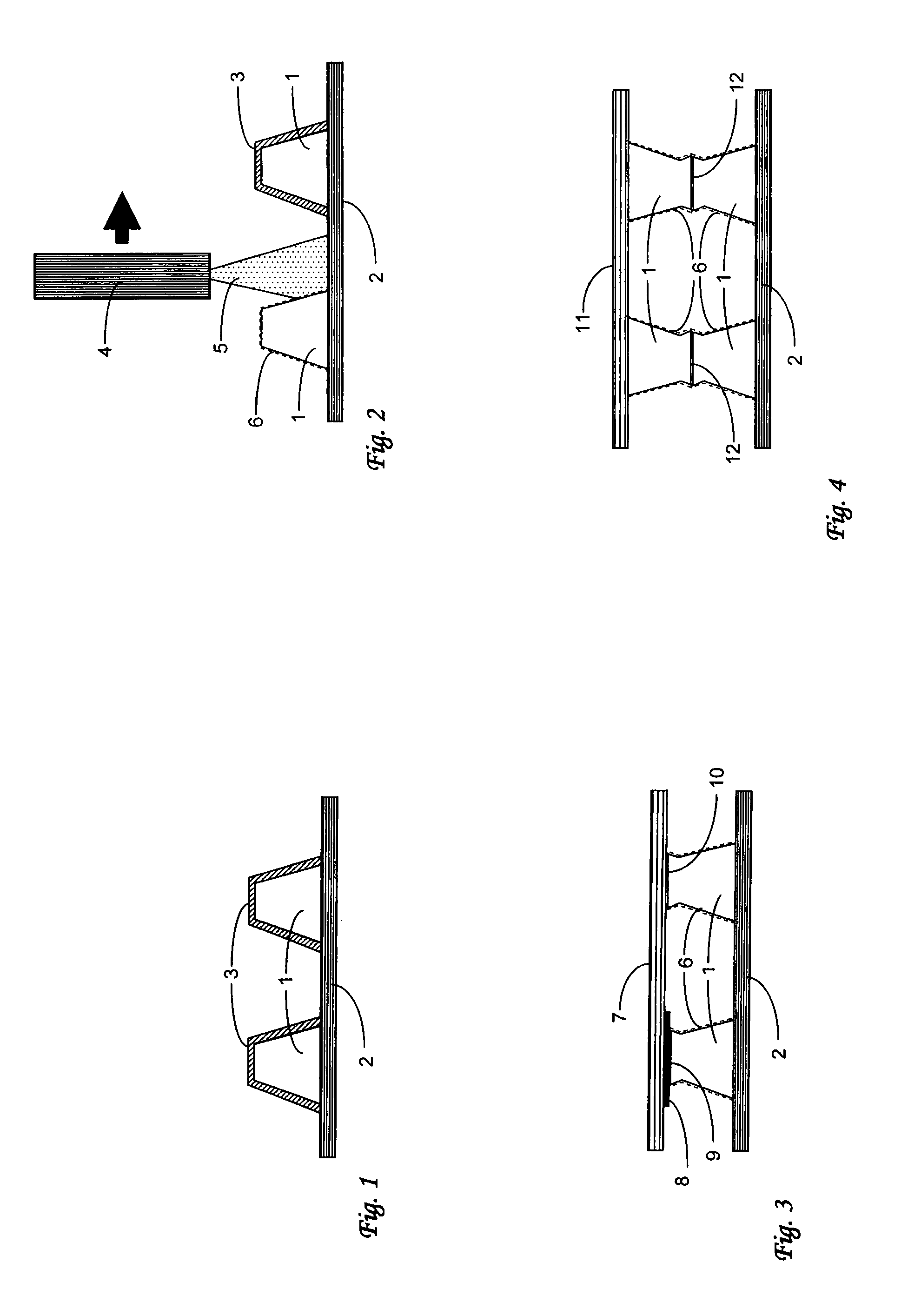
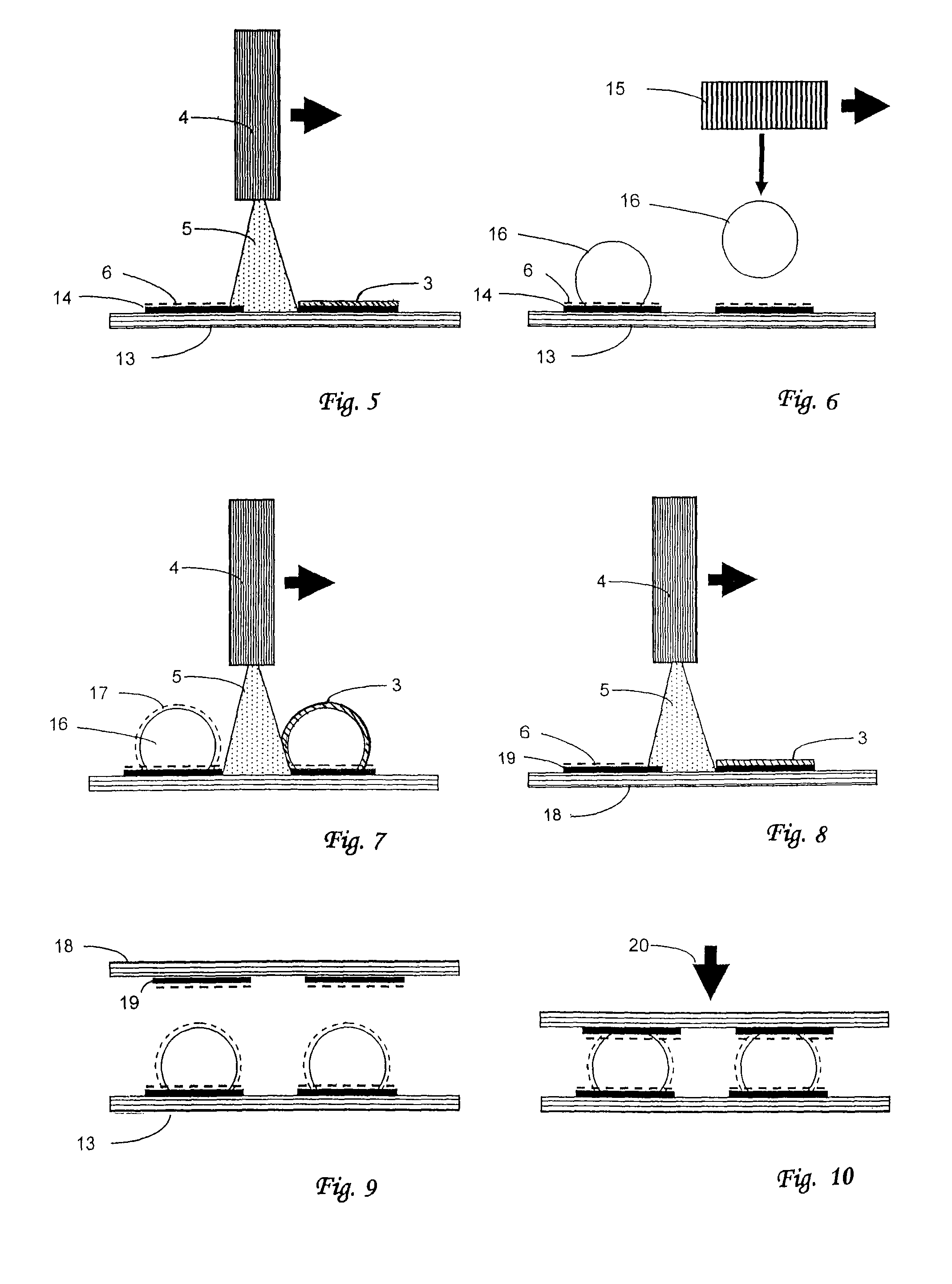
[0022]The present invention relates to a method for preparing and bonding surfaces, such as metallic contacts, by the sequential or concurrent application of a reducing agent and a passivation agent to remove an oxidation layer from the surfaces and then generate a passivated layer on the surfaces to prevent the subsequent formation of oxides on the surfaces. For purposes of the present invention and the following descriptions of the invention, an “agent”, such as a reducing agent or a passivation agent, is defined as a member, or species, of one or more groups, or genuses, of elements, chemicals or chemical compounds or mixtures thereof in a gaseous form suitable for application to the surfaces to be treated and providing the desired effect on the surfaces to be treated, such as the removal of oxides from the surfaces or the passivation of the surfaces to prevent the subsequent formation of oxides thereon.

[0023]FIG. 1 shows an array of metallic contacts 1 situated on a substrate 2....


PUM

PropertyMeasurementUnit
temperatureaaaaaaaaaa
poweraaaaaaaaaa

Abstract

A method of removing oxidation from certain metallic contact surfaces utilizing a combination of relatively simple and inexpensive off-the-shelf equipment and specific chemistry. The method being a very rapid dry process which does not require a vacuum or containment chamber, or toxic gasses / chemicals, and does not damage sensitive electronic circuits or components. Additionally, the process creates a passivation layer on the surface of the metallic contact which inhibits further oxidation while allowing rapid and complete bonding, even many hours after surface treatment, without having to remove the passivation layer. The process utilizes a room-ambient plasma applicator with hydrogen, nitrogen, and inert gasses.

Description

[0001]This application claims priority from U.S. Provisional Application No. 61 / 227,063 which was filed on Jul. 20, 2009.FIELD OF THE INVENTION[0002]This invention relates to the interconnect bonding of electrical, optical and / or mechanical components to form a three-dimensional multi-chip hybrid assembly. More specifically, it relates to the surface preparation of metallic contacts on the surface of flip-chip components to improve process throughput, yield, and reliability of the subsequent electrical and / or mechanical connection.BACKGROUND OF THE INVENTION[0003]Metallic contact flip-chip interconnect bonding has been successfully used for many years to provide mechanical and / or electrical connection between two or more electrical, optical, and-or mechanical components. An example of the flip-chip interconnect would be the face-to-face indium bump bonding of an optical detector chip to its corresponding readout integrated circuit (ROIC) chip to form an infrared detector focal plane...

Claims


Application Information

Patent Timeline
Patent Type & Authority Patents(United States)
IPC IPC(8): B23K35/38B23K31/02H01L21/44
CPCH01L24/11H01L24/81B23K1/20B32B38/0008B32B2310/14B32B2457/00H01L24/13H01L24/16H01L2224/11831H01L2224/13099H01L2224/16H01L2224/81054H01L2224/81191H01L2224/81193H01L2224/812H01L2224/81801H01L2924/01013H01L2924/01022H01L2924/01029H01L2924/0103H01L2924/01032H01L2924/01047H01L2924/01049H01L2924/01051H01L2924/01073H01L2924/01079H01L2924/01082H01L2924/14H01L2924/01006H01L2924/01033H01L2924/01042H01L2924/0105H01L2924/01074H01L2924/01075H01L2924/014H01L2224/131H01L2224/136H01L2924/00014H01L2224/81011H01L2224/81013H01L2924/0001H01L2224/11334H01L2224/0381
Inventor SCHULTE, ERIC FRANK
Owner ONTOS EQUIP SYST
Why Eureka
Try Eureka