Photodetector with internal gain and detector comprising an array of such photodetectors

a photodetector and photodetector technology, applied in the field of photodetectors with internal gain, can solve the problems of low quantum efficiency (generally less than 50%), limited detection wavelength range, bulky photocathode detectors, etc., and achieve low bias voltage, good signal-to-noise ratio, and high gain amplification

Active Publication Date: 2013-11-26
COMMISSARIAT A LENERGIE ATOMIQUE ET AUX ENERGIES ALTERNATIVES
View PDF5 Cites 0 Cited by
  • Summary
  • Abstract
  • Description
  • Claims
  • Application Information

AI Technical Summary

Benefits of technology

[0015]The object of the present invention is to propose a photodetector with internal gain which is capable of achieving high gain amplification at low bias voltages and which has a good signal-to-noise ratio, a low response time and a low tunneling current over a wide range of detected wavelengths up to 20 micrometers.

Problems solved by technology

Although they have a good signal-to-noise ratio, photocathode detectors are usually bulky, are limited in terms of their detectable wavelength range (usually less than 1.7 micrometers) and have a low quantum efficiency (generally less than 50%).
The quantum efficiency of EMCCD devices is generally high for wavelengths in the visible spectrum but deteriorates rapidly in the near infrared spectrum.
In addition, the spectral sensitivity of this type of device is limited by the material which is used for the CCD arrays, this is usually Si which has an energy gap which corresponds to a cut-off wavelength of 0.9 micrometer.
APDs made of Si or of a Group III-V type semiconductor such as diodes made using InGaAs, for example, operate at ambient temperature, but their performance is limited by the presence of impact ionization which is produced by both the electrons and holes.
At high gain, there is thus considerable deterioration of the signal-to-noise ratio as well as considerable deterioration of the response time.
Avalanche breakdown can also occur; this makes APDs of this type non-linear.

Method used


Image

  • Photodetector with internal gain and detector comprising an array of such photodetectors
  • Photodetector with internal gain and detector comprising an array of such photodetectors
  • Photodetector with internal gain and detector comprising an array of such photodetectors

Examples


first embodiment

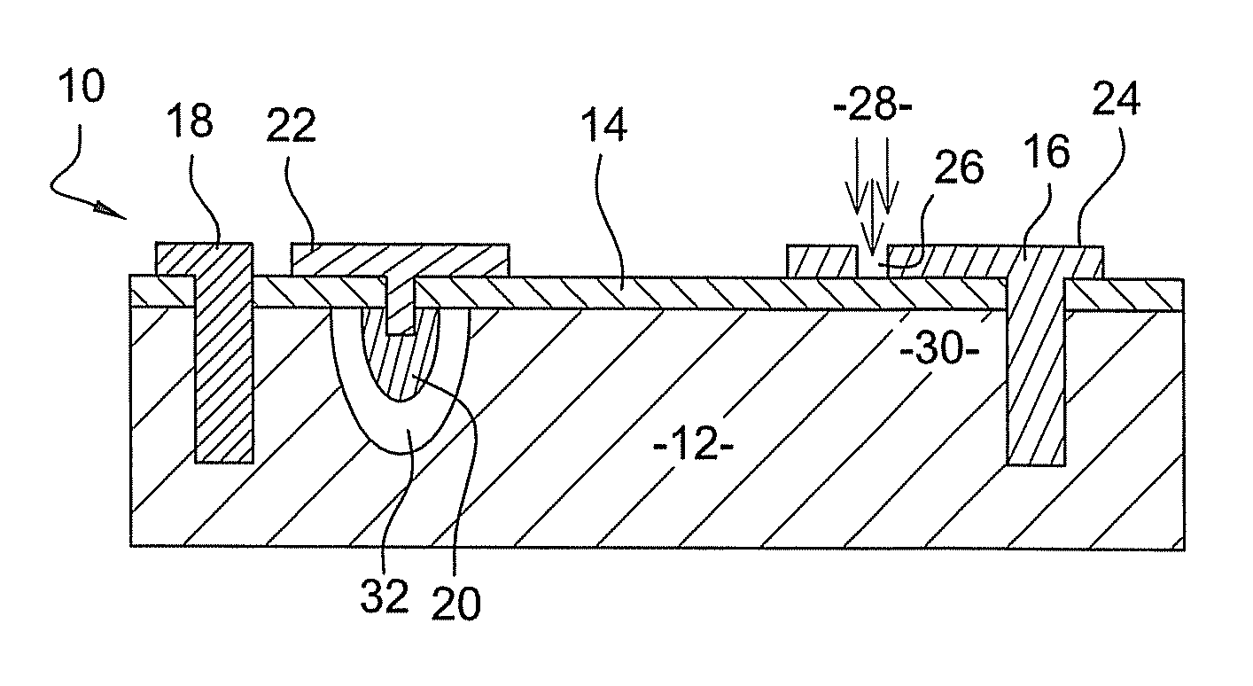
[0061]FIGS. 1 and 2 are schematic views of a photodetector with internal gain 10 in accordance with a

[0062]Photodetector 10 comprises semiconductor layer 12 of a first conductivity type, for example P-type conductivity, and a passivation layer 14, made of zinc sulfide (ZnS) for instance, which covers layer 12 and protects it against chemical, mechanical and electrical damage. Two metallic (preferably ohmic) contacts 16, 18, such as gold, for example, are also provided in layer 12; they pass through passivation layer 14 and emerge on the surface of the passivation layer.

[0063]Layer 12 is made of a semiconductor material doped with nearby majority charge carriers which do not produce impact ionization events. Thus, when this layer is subjected to an electric field, only the minority charge carriers—electrons in the case of P-type conductivity—produce impact ionization events. A CdxHg1-xTe alloy with a stoichiometric Cd composition of less than 60% (x<0.6) makes it possible to obtain t...

third embodiment

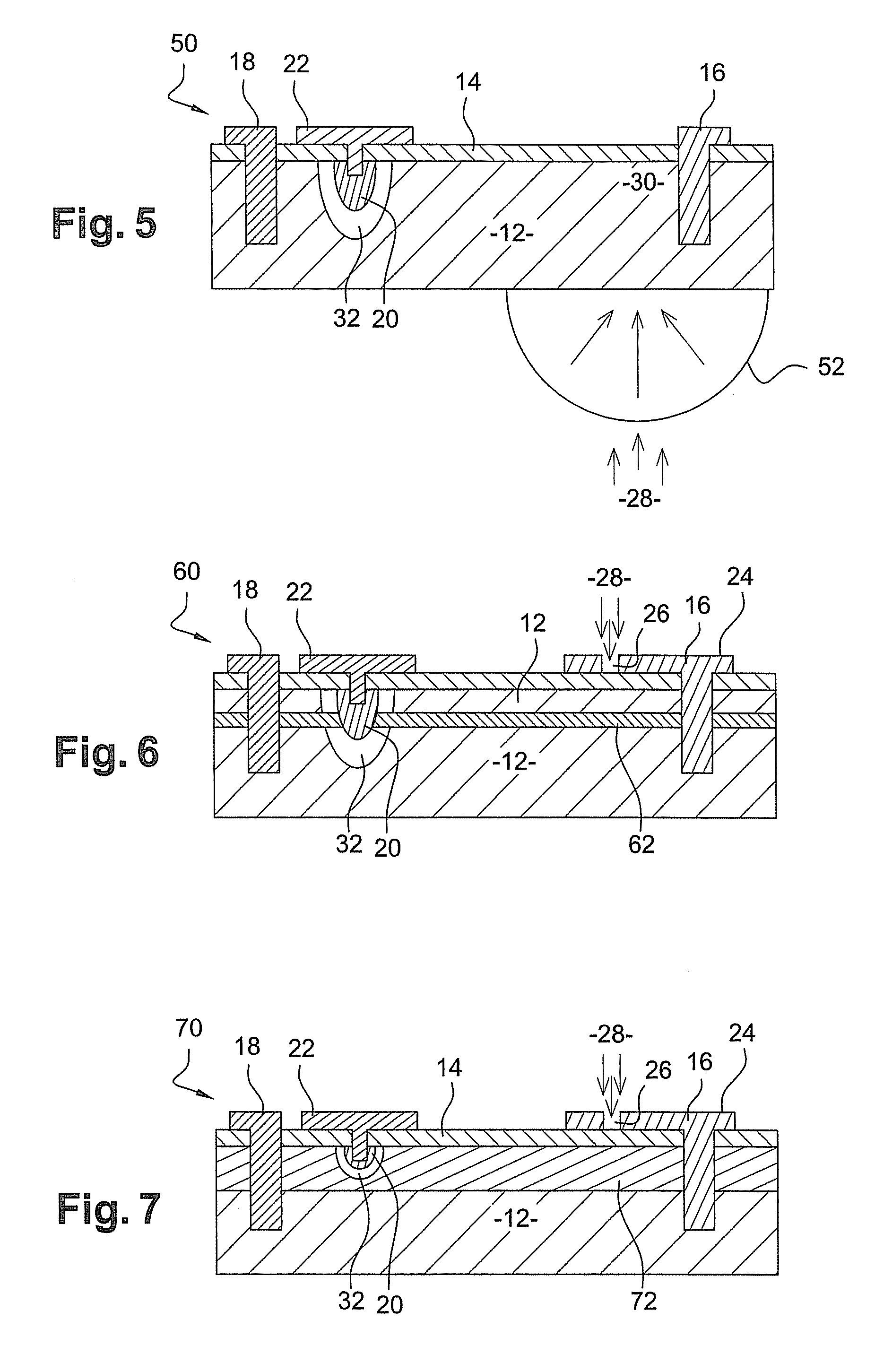
[0079]FIG. 5 is a schematic cross-sectional view of a third embodiment in which photodetector 50 is illuminated from the rear by electromagnetic radiation 28 and is provided with a micro lens 52 which focuses radiation 28 onto photon collection region 30. The surface area of biasing contact 16 is also reduced, for the reasons stated earlier. Note that the lens is positioned on the back face of layer 12, preferably opposite contact 16. This positioning makes it possible to concentrate the absorption of light in the vicinity of contact 16.

[0080]FIG. 6 schematically shows a cross-sectional view of a fourth embodiment of the invention. This embodiment differs from the preceding embodiments in that semiconductor layer 62 is inserted into semiconductor layer 12 at the level of region 20 of the P-N junction. This layer 62 is either of the same type of conductivity as layer 12, for example p-type conductivity, or of an opposite conductivity type with less doping and has a band gap which is ...

fifth embodiment

[0084]FIG. 7 schematically shows a cross-sectional view of the invention. This embodiment differs from the embodiments in FIGS. 1 to 5 in that semiconductor layer 72 having the same type of conductivity as layer 12, but with a larger band gap than that of layer 12, is inserted between the latter and passivation layer 14. Layer 72 is also sufficiently thick for depletion zone 32 to be formed entirely within this layer with a low reverse bias value and through this layer for higher reverse bias values. The thickness of layer 72 depends on the type of doping and is preferably 0.5 μm to 1 μm more than the depth of region 20. Layer 72 preferably consists of CdxHg1-xTe with a higher x composition than the x composition of layer 12. For example, layer 12 has an x composition of 0.15 to 0.4, preferably an x composition equal to 0.3 and layer 72 has an x composition of 0.2 to 0.5, preferably an x composition equal to 0.35.

[0085]Note that zone 32 only extends into layer 12 with high reverse b...


PUM


Abstract

A photodetector with internal gain comprising a semiconductor structure in which impact ionization events are produced mostly by minority charge carriers; a first biasing contact and a second biasing contact located in the semiconductor structure; a means of defining, in the semiconductor structure, a photon collection region close to first biasing contact; a P-N type junction formed in the semiconductor structure between the two biasing contacts and close to the second biasing contact; and a collector contact which is located in the P-N junction and used to collect current in the P-N junction.

Description

BACKGROUND OF THE INVENTION[0001]1. Field of the Invention[0002]The invention relates to the field of photodetectors with internal gain.[0003]2. Description of the Related Art[0004]A photodetector with internal gain is a device which detects electromagnetic radiation and generates an electrical signal, said signal being amplified before it is processed by proximity electronics used to convert, amplify and / or digitize the signal produced by the photodetector.[0005]The internal amplification of the photodetector makes it possible to reduce the amplification of the proximity electronics which is usually a source of noise. In addition, a photodetector with internal gain is currently the only device which is capable of quickly detecting a small number of photons; it is also the only device which allows accurate photon counting.[0006]There are several types of photodetectors with internal gain, in particular photocathode detectors, electron-multiplier charge-coupled devices, avalanche pho...

Claims


Application Information

Patent Timeline
Patent Type & Authority Patents(United States)
IPC IPC(8): H01L27/144
CPCH01L31/09H01L31/107
Inventor ROTHMAN, JOHANCHAMONAL, JEAN-PAUL
Owner COMMISSARIAT A LENERGIE ATOMIQUE ET AUX ENERGIES ALTERNATIVES
Why Eureka
Try Eureka