Diffusion barrier and etch stop films

a technology of diffusion barrier and stop film, which is applied in the direction of basic electric elements, semiconductor/solid-state device manufacturing, electric apparatus, etc., can solve the problems of reducing the power consumption of complex integrated circuits, lack of suitable mechanical and electrical characteristics of low-k materials, etc., and achieve the effect of preventing undesirable oxidation of metal surfaces

Active Publication Date: 2014-03-11
NOVELLUS SYSTEMS
View PDF180 Cites 30 Cited by
  • Summary
  • Abstract
  • Description
  • Claims
  • Application Information

AI Technical Summary

Benefits of technology

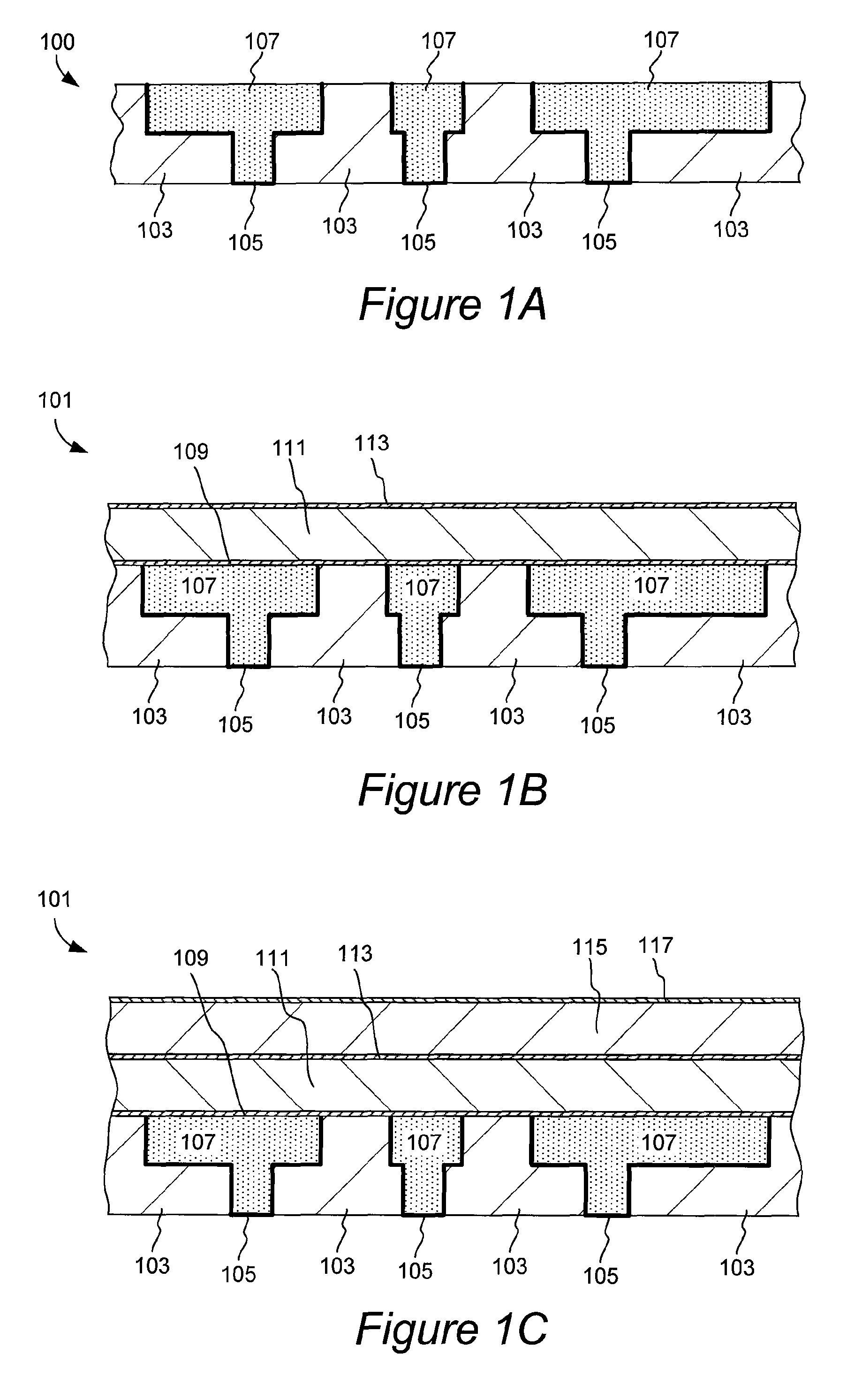
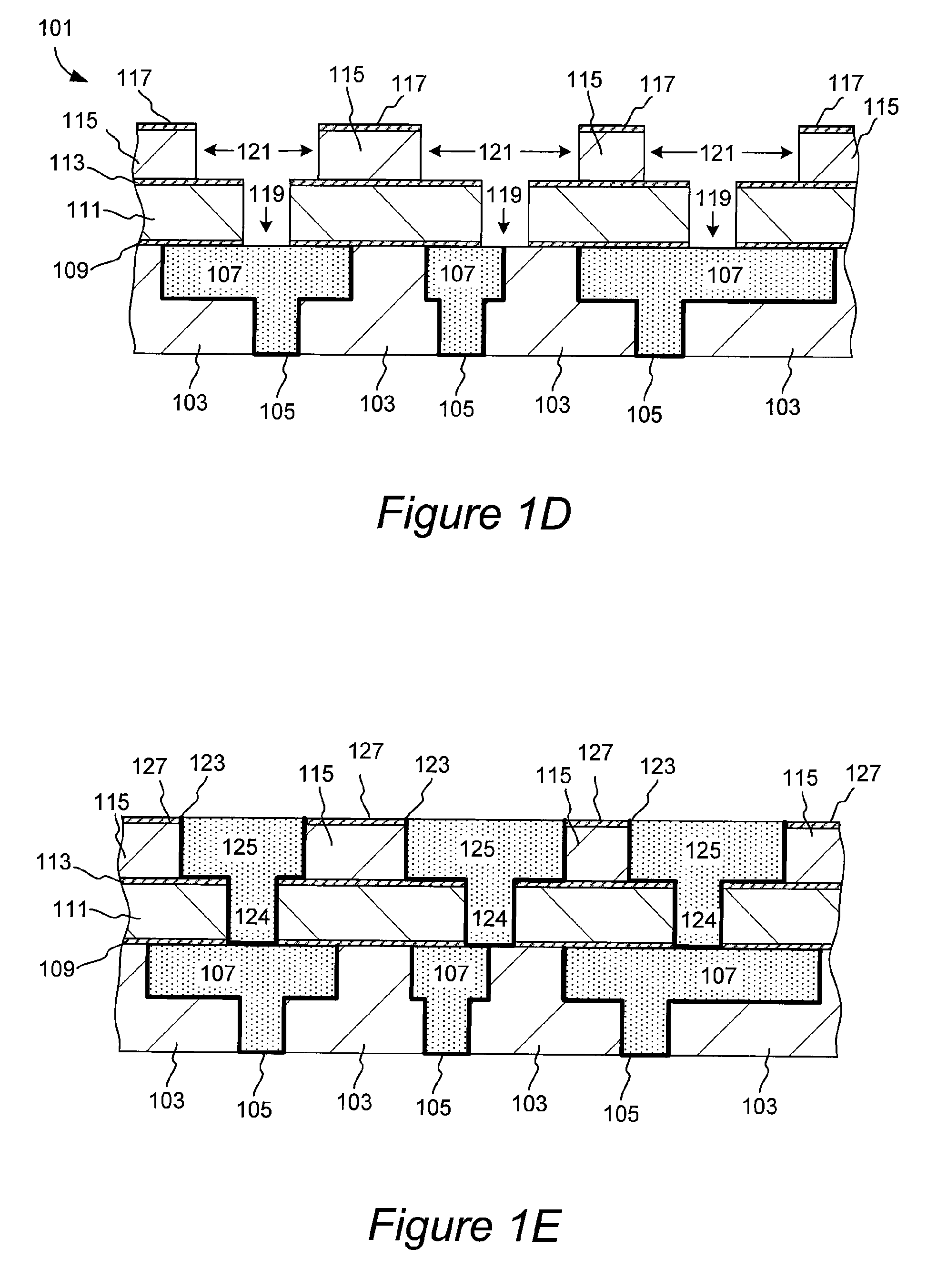
[0008]One of such desirable properties is hermeticity. Films having high hermeticity and a low dielectric constant are herein provided. These films can be employed in a variety of applications in integrated circuit (IC) fabrication that require such combination of properties. These films are particularly suitable for use as copper diffusion barrier films, etch stop films, CMP stop films and other hardmasks used during semiconductor processing. Hermetic low-k films can protect the underlying layers, such as layers of metal and dielectric, from exposure to atmospheric moisture and oxygen, thereby preventing undesirable oxidation of metal surfaces and absorption of moisture by a dielectric. In certain embodiments, the hermetic films described herein substantially prevent penetration of any or all of ambient atmospheric components including moisture, oxygen, carbon dioxide and nitrogen. In particular embodiments, the hermetic films act as barriers to at least atmospheric moisture and / or oxygen.
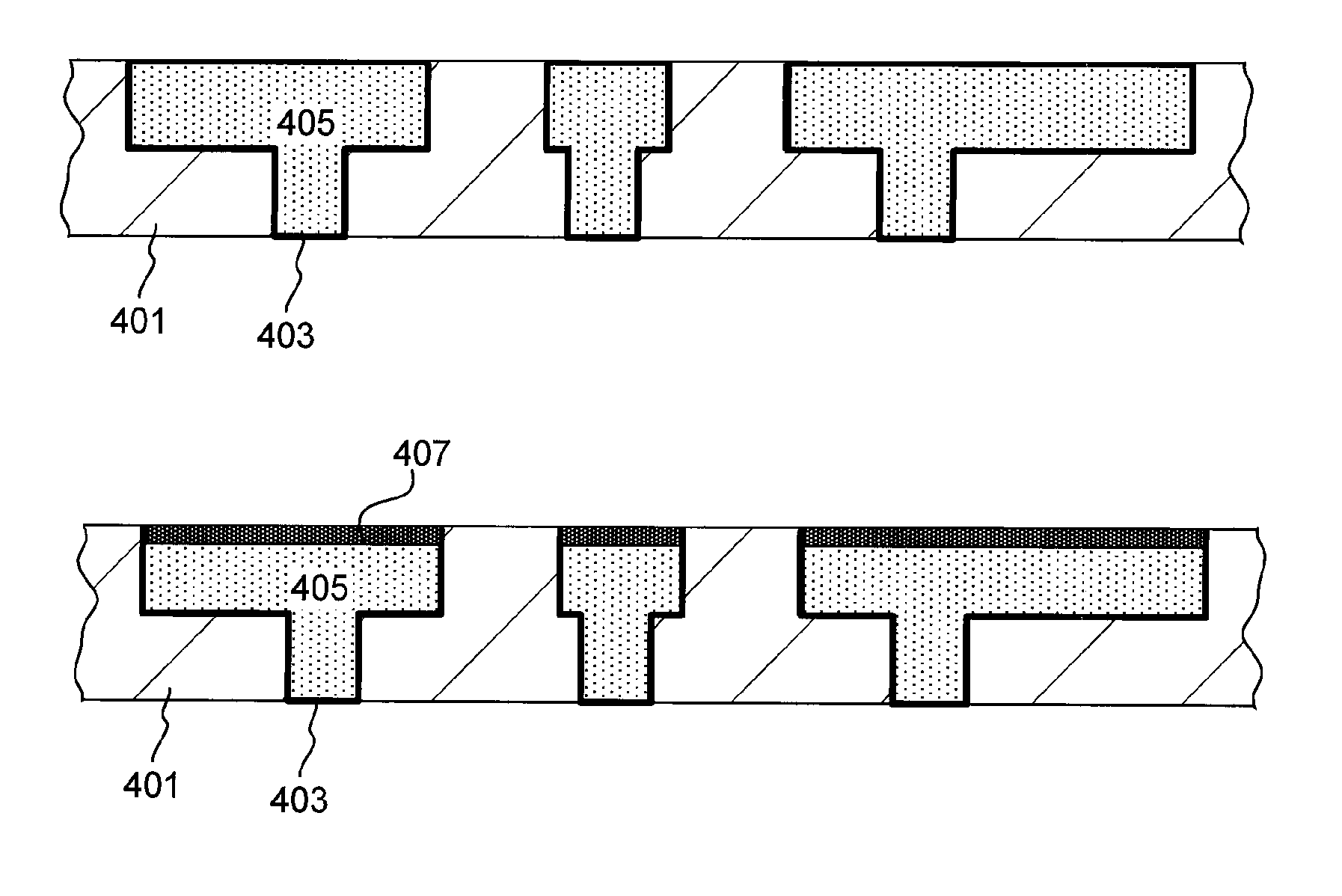
[0009]Specifically, a bi-layer film having a hermetic bottom layer composed of hydrogen doped carbon and a low dielectric constant (low-k) top layer composed of low-k silicon carbide (e.g., high carbon content hydrogen doped silicon carbide) can be employed. Such bi-layer film can be deposited by PECVD methods on a partially fabricated semiconductor substrate having exposed layers of dielectric and metal. In some embodiments, the top portions of exposed metal lines or interconnects are converted to protective self-aligned buffer (PSAB) layers prior to formation of the bi-layer barrier in order to improve adhesion and to reduce the possibility of inadvertent oxidation of metal surfaces and metal electromigration.
[0015]In some embodiments, the copper diffusion barrier film stack is provided, at least in part, on a protective self-aligned buffer (PSAB) layer comprising material selected from the group consisting of CuxSiy, CuxPy, CuxBy, CuxGey, CuxAsy, CuxCy and copper chalcogenides (e.g., CuxSy, CuxSey, CuxTey). The PSAB layer resides on top of copper metal of the copper lines and serves to promote adhesion between the diffusion barrier film and the copper line. The PSAB layers also reduce electromigration during end use of IC devices.
[0016]The PSAB layer material can be further doped in some embodiments with nitrogen or carbon. Further, in some embodiments, a chemical reaction may occur during the doping operation, in which the first formed PSAB layer, e.g., copper silicide layer is partially or completely chemically transformed. For example, the copper silicide layer may be transformed to copper metal impregnated with silicon nitride or silicon carbide. In this example, the PSAB layer may be viewed as a very thin layer of silicon nitride or silicon carbide, located at the top portion of a copper line on the interface with the diffusion barrier film. The PSAB layer typically has a graded composition, with the silicon nitride concentration decreasing as the distance from the diffusion barrier interface increases. Such blended composition of the PSAB capping layer promotes excellent adhesion between the copper line and the diffusion barrier film.
[0023]PSAB layer can be formed, in some embodiments, by using a plasma enhanced chemical vapor deposition PECVD process. The PSAB layer can be formed at a temperature of less than about 300° C. Such low-temperature regime is advantageous in some embodiments, because higher temperatures may cause increased diffusion of copper silicide deeper into the copper line, thereby increasing its resistance.

Problems solved by technology

Further, the use of a low k material as an interlayer dielectric reduces the power consumption of complex integrated circuits.
The challenges related to etch stop and barrier layer integration stem from the lack of low-k materials possessing suitable mechanical and electrical characteristics.

Method used


Image

  • Diffusion barrier and etch stop films
  • Diffusion barrier and etch stop films
  • Diffusion barrier and etch stop films

Examples


examples

[0115]Formation of hermetic diffusion barrier films with a dielectric constant of less than about 4 will be illustrated by several specific examples. FIG. 7 illustrates a simulation plot of effective dielectric constant of a bi-layer diffusion barrier film as a function of thickness of the top low-k silicon carbide layer. The total thickness of the diffusion barrier bilayer film having a bottom hermetic hydrogen-doped carbon layer and a top low-k silicon carbide layer is 350 Å in this example. Dielectric constant of hydrogen-doped carbon material provided in this illustration is about 4.2, while dielectric constant of the low-k silicon carbide material in this example is 3.5. Depending on relative thicknesses of the constituent layers, the bi-layer film may have an effective dielectric constant ranging from about 3.5 to 4.2. Preferably, bi-layer films with a dielectric constant less than about 4.0 should be used as diffusion barriers. Referring to the example, illustrated in FIG. 7,...


PUM

PropertyMeasurementUnit
dielectric constantaaaaaaaaaa

Abstract

Films having high hermeticity and a low dielectric constant can be used as copper diffusion barrier films, etch stop films, CMP stop films and other hardmasks during IC fabrication. Hermetic films can protect the underlying layers, such as layers of metal and dielectric, from exposure to atmospheric moisture and oxygen, thereby preventing undesirable oxidation of metal surfaces and absorption of moisture by a dielectric. Specifically, a bi-layer film having a hermetic bottom layer composed of hydrogen doped carbon and a low dielectric constant (low-k) top layer composed of low-k silicon carbide (e.g., high carbon content hydrogen doped silicon carbide) can be employed. Such bi-layer film can be deposited by PECVD methods on a partially fabricated semiconductor substrate having exposed layers of dielectric and metal.

Description

CROSS-REFERENCE TO RELATED APPLICATIONS[0001]This application is a divisional application claiming priority from U.S. patent application Ser. No. 11 / 710,652 filed Feb. 22, 2007, titled “Improved Diffusion Barrier and Etch Stop Films”, naming Yu et al. as inventors, which is incorporated herein by reference in its entirety for all purposes.FIELD OF THE INVENTION[0002]This invention relates to low dielectric constant films with hermetic properties for use in various applications. The invention also relates to methods of forming low dielectric constant films with improved performance in a wide range of VLSI and ULSI fabrication operations.BACKGROUND OF THE INVENTION[0003]There is a general need for materials with low dielectric constants (low-k) in the integrated circuit manufacturing industry. Using low-k materials as the interlayer dielectric (ILD) of conductive interconnects reduces the delay in signal propagation and signal crosstalk due to capacitive effects. The lower the dielect...

Claims


Application Information

Patent Timeline
Patent Type & Authority Patents(United States)
IPC IPC(8): H01L21/44
CPCH01L21/76829H01L21/76832H01L21/76834H01L21/76807H01L21/3212H01L21/76849H01L21/02274H01L21/76846H01L21/76867H01L21/02115H01L21/02167H01L21/02211H01L21/76855H01L21/311
Inventor YU, YONGSIKSUBRAMONIUM, PRAMODFANG, ZHIYUANHENRI, JONAPEN, ELIZABETHVITKAVAGE, DAN
Owner NOVELLUS SYSTEMS
Why Eureka
Try Eureka