Nanoneedle plasmonic photodetectors and solar cells

a plasmonic photodetector and nano-needle technology, applied in the field of nano-sized transducers, can solve the problems of difficult batch fabrication process, inability to integrate, and inability to grow direct-bandgap iii-v compound materials in thin-film growth, etc., and achieve the effect of improving device performan

Inactive Publication Date: 2014-08-19
RGT UNIV OF CALIFORNIA
View PDF19 Cites 14 Cited by
  • Summary
  • Abstract
  • Description
  • Claims
  • Application Information

AI Technical Summary

Benefits of technology

[0006]The present disclosure provides a new growth mode that produces group III-V nanostructures by means of metal organic chemical vapor deposition (MOCVD). In particular, this disclosure provides a catalyst-free growth mode of defect-free Gallium Arsenide (GaAs)-based nanostructures on silicon (Si) substrates with a complementary metal-oxide-semiconductor (CMOS)-compatible growth temperature of around 400° C. The nanostructures are crystalline, having a pure wurtzite phase crystal structure that is free of zincblende phases. The absence of zincblende phases is atypical for GaAs crystalline structures. However, it is important to note that an entire nanostructure need not have a pure crystalline structure to be usable in accordance with the present disclosure. Instead, it is preferred that a p-n junction formed with a portion of a nanostructure be a single phase crystalline structure for better device performances.
[0007]An embodiment of the present disclosure is a photodetector that is fabricated using a nanostructure in the form of a nanoneedle as a base structure. Each nanoneedle preferably has a sharp 2 to 5 nanometer (nm) tip, a 600 nm wide base and a 4 micrometer (μm) length. Thus, the preferred nanoneedles are substantially hexagonal needle-like crystal structures that assume a 6° to 9° tapered shape. The 600 nm wide base allows the typical micro-fabrication processes, such as optical lithography, to be applied. However, it is important to note that nanoneedles that are suitable for applications such as photodetectors may be grown to have a wide range of taper angles. An exemplary taper angle range for the disclosed nanoneedles is from 1° to 30°.

Problems solved by technology

Traditional thin-film growth of direct-bandgap III-V compound materials is not suitable for integration due to a high growth temperature above 600° C. and a high dislocation density when growing on Si.
However, while progress has been made in producing defect-free nanostructures on Si substrates at relatively low temperatures in the range of 430° C.-470° C., the use of metal catalysts such as gold (Au) raises concerns about fabricating such nanostructures using CMOS fabrication techniques.
Additionally, small and fragile nanostructure footprints such as those of thin nanowires have made it difficult to fabricate group III-V nanostructures through the use of optical lithography and batch fabrication processes.

Method used


Image

  • Nanoneedle plasmonic photodetectors and solar cells
  • Nanoneedle plasmonic photodetectors and solar cells
  • Nanoneedle plasmonic photodetectors and solar cells

Examples


Embodiment Construction

[0029]The embodiments set forth below represent the necessary information to enable those skilled in the art to practice the disclosure and illustrate the best mode of practicing the disclosure. Upon reading the following description in light of the accompanying drawing figures, those skilled in the art will understand the concepts of the disclosure and will recognize applications of these concepts not particularly addressed herein. It should be understood that these concepts and applications fall within the scope of the disclosure and the accompanying claims.

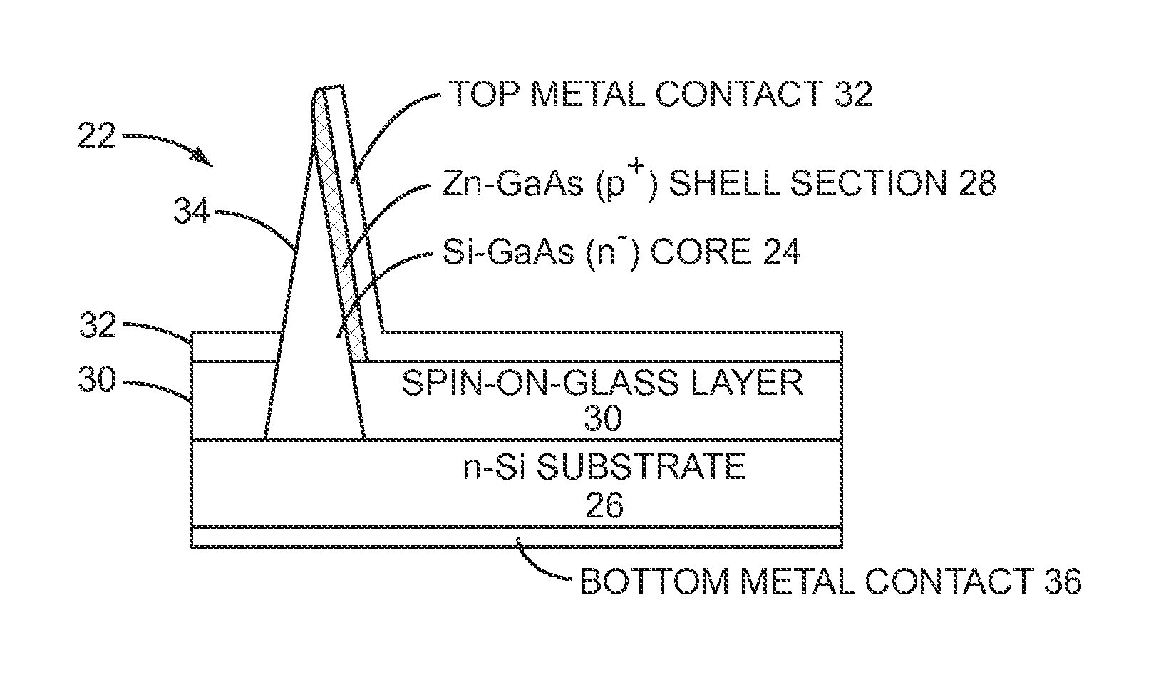
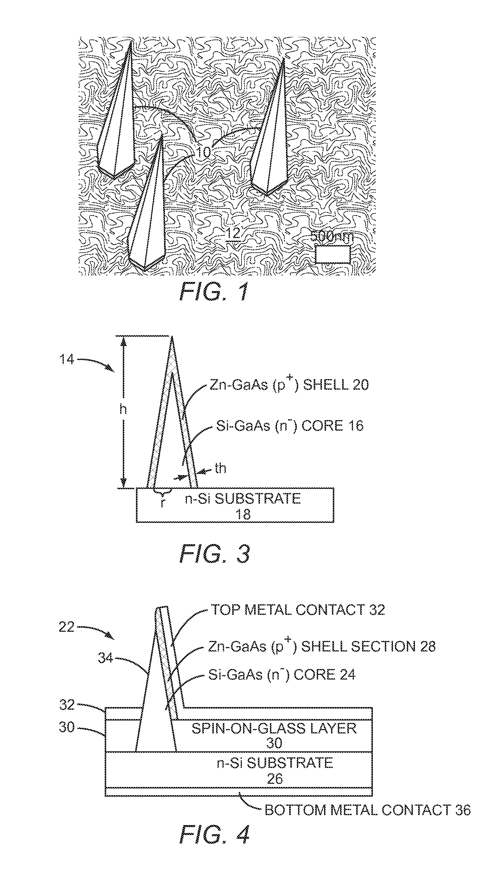
[0030]In an embodiment of the present disclosure, a Gallium Arsenide (GaAs)-based nanoneedle photodetector is monolithically grown and processed on a silicon (Si) substrate using a complementary metal-oxide-semiconductor (CMOS)-compatible catalyst-free and low-temperature (400° C.) crystal growth technique. Due to the catalyst-free nature of the crystal growth technique, there is no metal contamination of either the Si substrat...


PUM


Abstract

The present disclosure provides a catalyst-free growth mode of defect-free Gallium Arsenide (GaAs)-based nanoneedles on silicon (Si) substrates with a complementary metal-oxide-semiconductor (CMOS)-compatible growth temperature of around 400° C. Each nanoneedle has a sharp 2 to 5 nanometer (nm) tip, a 600 nm wide base and a 4 micrometer (μm) length. Thus, the disclosed nanoneedles are substantially hexagonal needle-like crystal structures that assume a 6° to 9° tapered shape. The 600 nm wide base allows the typical micro-fabrication processes, such as optical lithography, to be applied. Therefore, nanoneedles are an ideal platform for the integration of optoelectronic devices on Si substrates. A nanoneedle avalanche photodiode (APD) grown on silicon is presented in this disclosure as a device application example. The APD attains a high current gain of 265 with only 8V bias.

Description

RELATED APPLICATIONS[0001]This application claims the benefit of provisional patent application Ser. No. 61 / 181,494, filed May 27, 2009, the disclosure of which is hereby incorporated herein by reference in its entirety.GOVERNMENT RIGHTS[0002]This invention was made with government funds under Contract No. HR0011-07-3-0002 awarded by DARPA. The U.S. Government has rights in this invention.FIELD OF THE DISCLOSURE[0003]The present disclosure relates to nano-sized transducers for converting light radiation into a photocurrent and / or photovoltage.BACKGROUND OF THE DISCLOSURE[0004]An important goal of the electronics industry is an integration of optoelectronic devices with silicon (Si) substrates through the use of traditional complementary metal-oxide-semiconductor (CMOS) fabrication techniques. It is particularly desirable to develop a means for monolithic heterogeneous integration of direct-bandgap III-V compound materials onto Si CMOS substrates. For example, many important and long...

Claims


Application Information

Patent Timeline
Patent Type & Authority Patents(United States)
IPC IPC(8): H01L31/072H01L31/18H01L31/06
CPCY02E10/544H01L31/072H01L31/0522Y02E10/52H01L31/1852Y10S977/954H01L31/0304B82Y15/00H01L31/1844H01L31/054H01L31/03529Y10S977/90
Inventor CHUANG, CHIH-WEICHANG-HASNAIN, CONNIESEDGWICK, FORREST GRANTKO, WAI SON
Owner RGT UNIV OF CALIFORNIA
Why Eureka
Try Eureka