

Antireflective coating composition and process thereof
a technology of coating composition and anti-reflective coating, applied in the direction of photosensitive materials, instruments, photomechanical equipment, etc., can solve the problems of back reflectivity, thin film interference effect and reflective notching, and change in critical line width dimensions
- Summary
- Abstract
- Description
- Claims
- Application Information
AI Technical Summary
Benefits of technology
Problems solved by technology
Method used
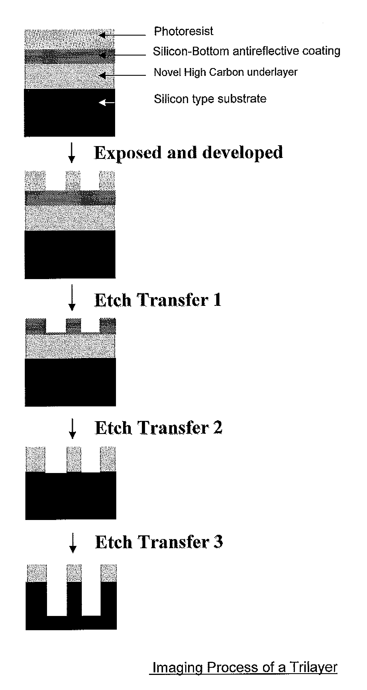
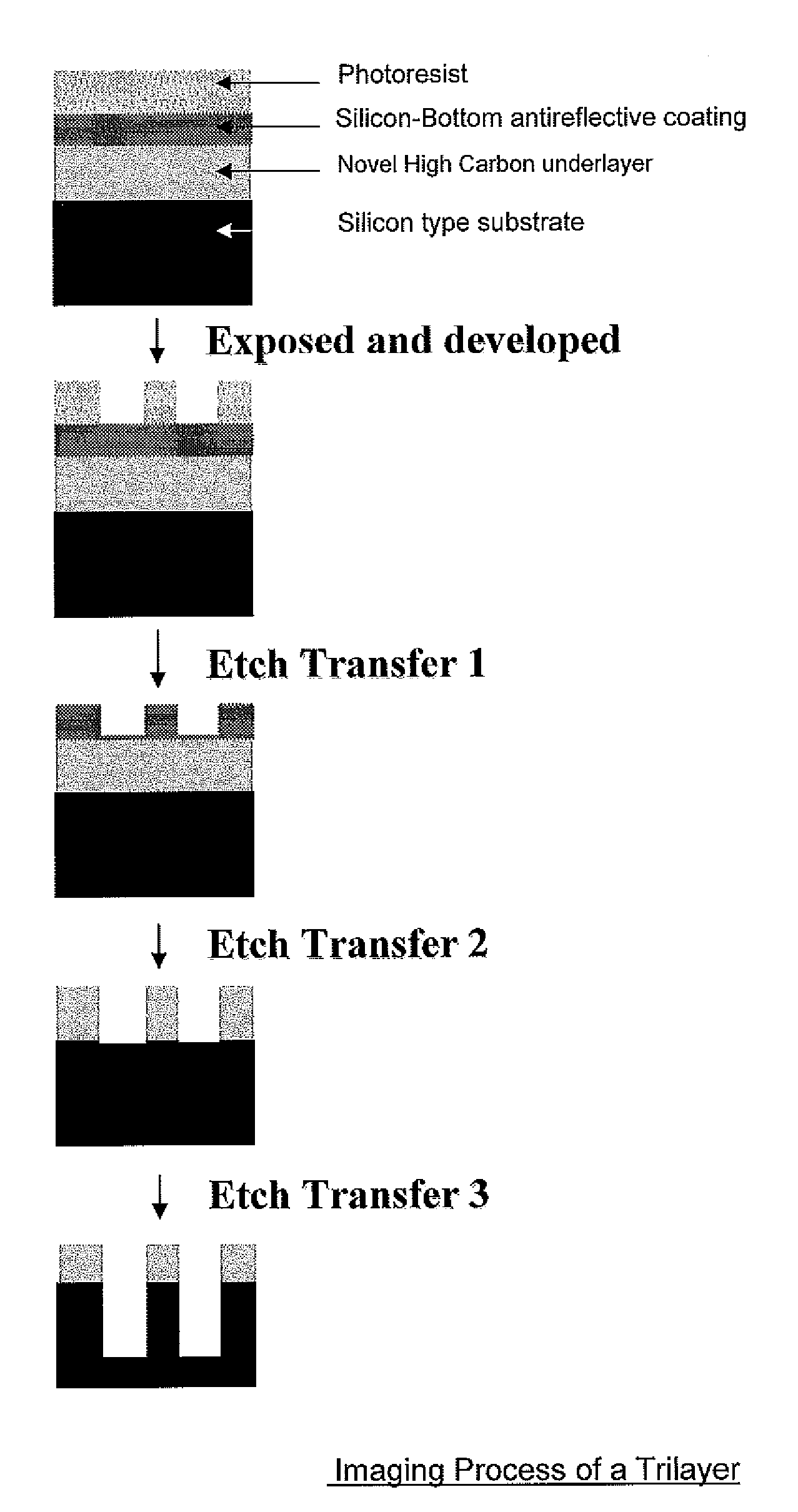
Image

Examples
example 1
Synthesis of Copolymer of 2-phenylphenol / divinylbenzene / a-anthracenemethanol
[0064]A solution was prepared consisting of 12.76 g (0.075 mol) 2-phenylphenol, 15.62 g (0.075 mol) 9-Anthracene Methanol, 9.76 (0.075 mol) divinylbenzene dissolved in 25 g cyclopepentyl methyl ether (CPME) and 90 g diethylelene glycol dimethyl ether (DEGME) and the mixture was stirred for 5 minutes in a 250 mL, 4 neck flask equipped with an overhead mechanical stirrer, condenser, thermo watch, Dean Stark trap and an N2 purge. After this time, 1.14 g of triflic acid (3% wt of monomers) was added to the stirred mixture and it was stirred for another 5 minutes. The temperature of the stirred mixture was then raised to 140° C. and heated for 3 hours. After cooling the reaction mixture and diluting it with 250 mL of CPME, it was transferred to a separatory funnel, and it was washed with two aliquots of deionised (DI) water (2×200 mL). The polymer was precipitated by drowning into hexane. The polymer was filtered...
example 2
[0065]The polymer of Example 1 was dissolved in PGMEA as a 7% wt solution. This solution was filtered through a 0.2 μm PTFE filter and the solution was applied to silicon water and spun at 1,500 rpm to form a 200 micron thick polymer film. The coating quality of this polymer from a spin casting solvent was good with no visible defects present. Prior to post-applied bake (PAB), the coating passed an edgebead removal (EBR) test with PGMEA showing clean removal of polymer at the water's edge where the PGMEA solvent was applied. After PAB (230° or 400° C.), the coatings passed a soak tests with PGMEA solvent showing no visible sign of any film thickness loss. After PAB processing at different temperatures the polymer showed the following elemental composition.
[0066]
230° bake400° bake% C89.6480.88% H5.923.72% O2.828.72
With a PAB of 250° C. this polymer coating gave n=1.47 and k=0.68 Six additional batches were made of this material including one which was scaled up tenfold. All...
example 3
Synthesis of Co Polymer of 2-phenylphenol / divinylbenzene / a-anthracenemethanol
[0067]Using the same setup as described for Example 1, 8.50 g (0.06 mol) 2-phenylphenol, 30.34 g(0.15 mol) 9-anthracene methanol, 13.0 g (0.10 mol) divinylbenzene, 45 g CPME and 160 g DEGME were used. As in Example 1, after stirring this solution for 5 minutes, 1.55 g (3% wt of monomers) triflic acid was added and the reaction was stirred for another 5 minutes. As in example 1, the reaction temperature was increased to 140° C. and heated for 5 hours. After cooling the reaction mixture and diluting it with 250 mL of CPME, it was transferred to a separatory funnel, and it was washed with two aliquots of DI water (2×200 mL). The polymer was then precipitated into hexane. The polymer was then washed with hexane, air dried by suction and finally dried in a vacuum oven overnight. This process yielded 45% finished polymer from the starting materials. The weight average molecular weight of the polymer was 1,727 wit...
PUM
| Property | Measurement | Unit |
|---|---|---|
| temperature | aaaaa | aaaaa |
| mole % | aaaaa | aaaaa |
| refractive index | aaaaa | aaaaa |
Abstract
Description
Claims
Application Information