Semiconductor device for electron emission in a vacuum

a semiconductor diode and electron emission technology, which is applied in the direction of transit-tube cathodes, discharge tubes/lamp details, electrical apparatus, etc., can solve the problems of inability to achieve stable electron emission, inability to produce, and difficulty in achieving the effect of reducing the number of electrons, and improving the distribution of current in the componen

Active Publication Date: 2016-04-05
THALES SA
View PDF4 Cites 3 Cited by
  • Summary
  • Abstract
  • Description
  • Claims
  • Application Information

AI Technical Summary

Benefits of technology

[0046]Other aims are to improve the lifespan and reduce the bulk of the devices for emitting electrons into a vacuum.
[0053]In addition to the fact that it is not necessary to use such materials, a second advantage results from the implementation that we have prioritized. The method selected for heating the electron gas in the emission device according to the invention is in fact much more effective than that used for the thermionic cathodes because it is selective. Unlike these thermionic devices, not all of the material is heated, only the free carriers via the internal electrical field induced by the powering up of the diode. Electron temperatures of several tens of thousands of degrees are thus possible in materials with large band gap such as those belonging to the III-N family. The temperature of the network, determined by Joule's law, then remains lower than that of the electron gas by several orders of magnitude. This is why the term “cold cathode” is used, since the network is, in relation to the electrons emitted into the vacuum, much colder.
[0054]For its part, the choice of the NPN structure is dictated by the material. The P-type doping of this family of semiconductors is in fact much more difficult to produce than the N-type doping which is well controlled. The access resistance of N-doped layers is thus several orders of magnitudes lower than that of P-doped layers. The biasing of the device through exclusively N-doped layers, made possible with this type of stack according to the invention, improves the distribution of the current in the component and makes it possible to obtain a much more intense and spatially uniform emission than if one of the electrical contacts was taken on a P-doped layer. A gain of 3 to 4 orders of magnitude on the emitted current is expected with this method.
[0056]In order to optimize the electron emission, the N-doped layer situated on the surface of the stack will have to be thin and strongly doped. Typically, this layer will have to have a thickness of less than 50 nm and a doping greater than some 1018 cm−3. Ideally, the thickness and the doping thereof will be chosen in such a way that, when the component is biased in emission, the non-depleted part of this layer will be sufficiently thin to minimize the cooling of the electrons which pass through it but thick enough to avoid the lateral depolarization of the reverse-biased diode. To allow for the emission of the hot electrons, the electrical contact of the N-doped layer situated on the surface is pierced.

Problems solved by technology

Today's electron sources integrated in power microwave amplifier tubes use the thermoelectronic emission obtained by heating electron sources called thermionic cathodes, to temperatures in the vicinity of 1000° C. Because of the physical principle used, these cathodes are limited in terms of emitted electron current and of lifespan, and also include the drawback of taking a fairly long time, of the order of a minute, to obtain the stabilized emission of electrons when they are heated, or switched on.
Cesium oxide is, however, chemically unstable and the diode has to be made to work in a powerful vacuum to increase its lifespan.
Even in these conditions, the layer of oxide degrades too rapidly for the device to be able to be used in the tubes.
Furthermore, the maximum energy that the electrons can acquire is limited to the curvature of the bands in the vicinity of the surface and is, at best, of the order of the band gap of the materials used (typically less than 2 eV).
Most of the electrons cannot therefore acquire sufficient energy to be emitted into the vacuum and only a small fraction, the most energetic of the electron distribution, leaves the material, hence low emission efficiency.
However, the gain in emission obtained by lowering the electron affinity using the material placed on the surface is wiped out by the energy losses induced by the collisions of the hot electrons with the network of the metal passed through.
Given the semiconductors used, such devices have a very low emission efficiency.
To increase the emission of electrons, a layer of cesium oxide is also deposited on the emissive surface but, as in the first solution, the instability of this oxide limits the lifespan of these devices.
These two solutions have not however led to any applications, the Spindt cathodes undergoing an accelerated degradation under the effect of the ion bombardment generated by the intense electrical field prevailing at the summit of the cones, and the carbon nanotubes not emitting a sufficient current density (effective emitted current density of the order of 1 A / cm2).
The effective emissive surface is thus greatly reduced and represents no more than a small fraction of the total surface area of the transistor which results in a low emission efficiency.
None of the solutions described previously have to date made it possible to produce an electron source which is both reliable and intense enough to compete with the thermionic cathodes used today in the power tubes.

Method used


Image

  • Semiconductor device for electron emission in a vacuum
  • Semiconductor device for electron emission in a vacuum
  • Semiconductor device for electron emission in a vacuum

Examples


first embodiment

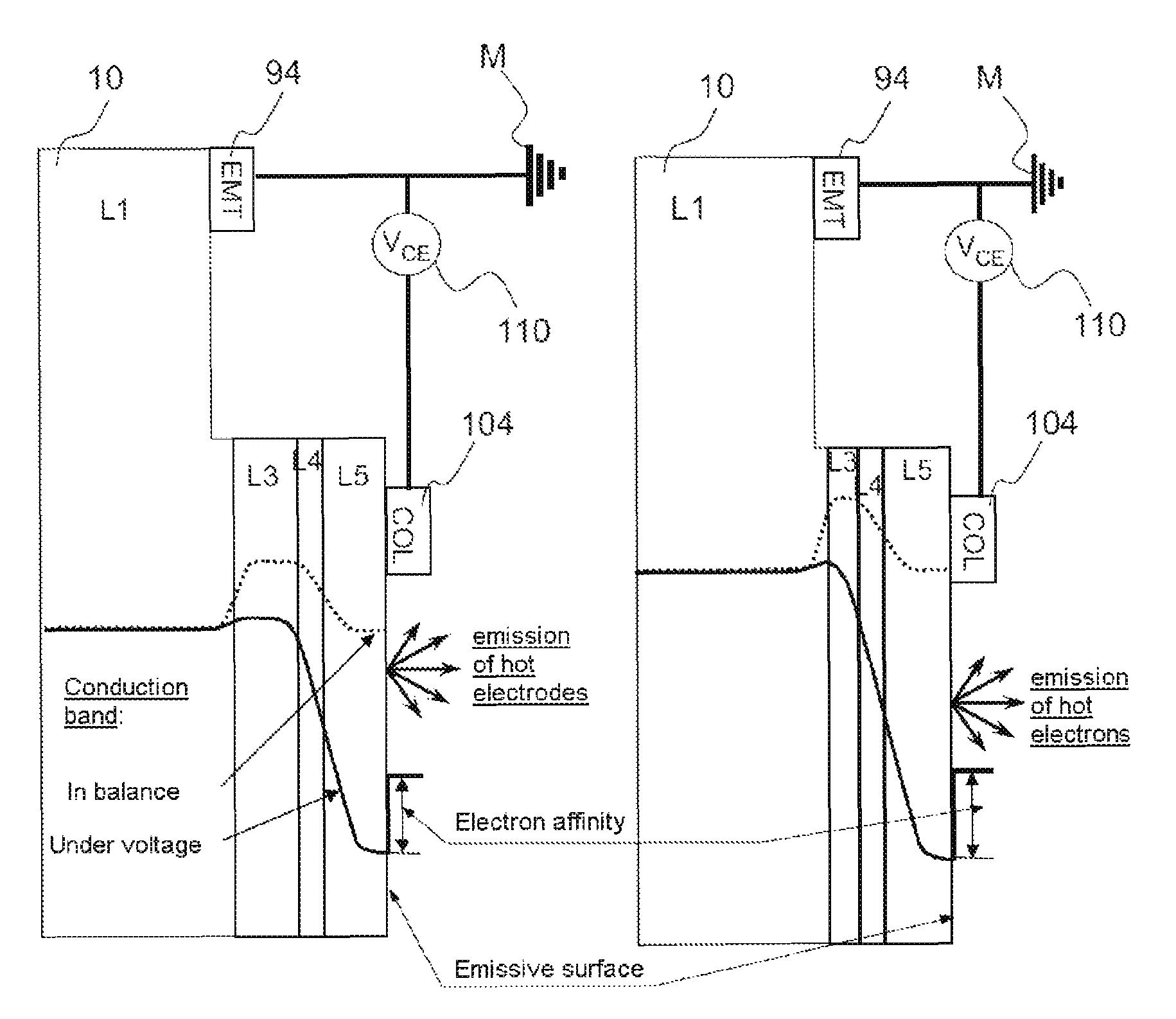
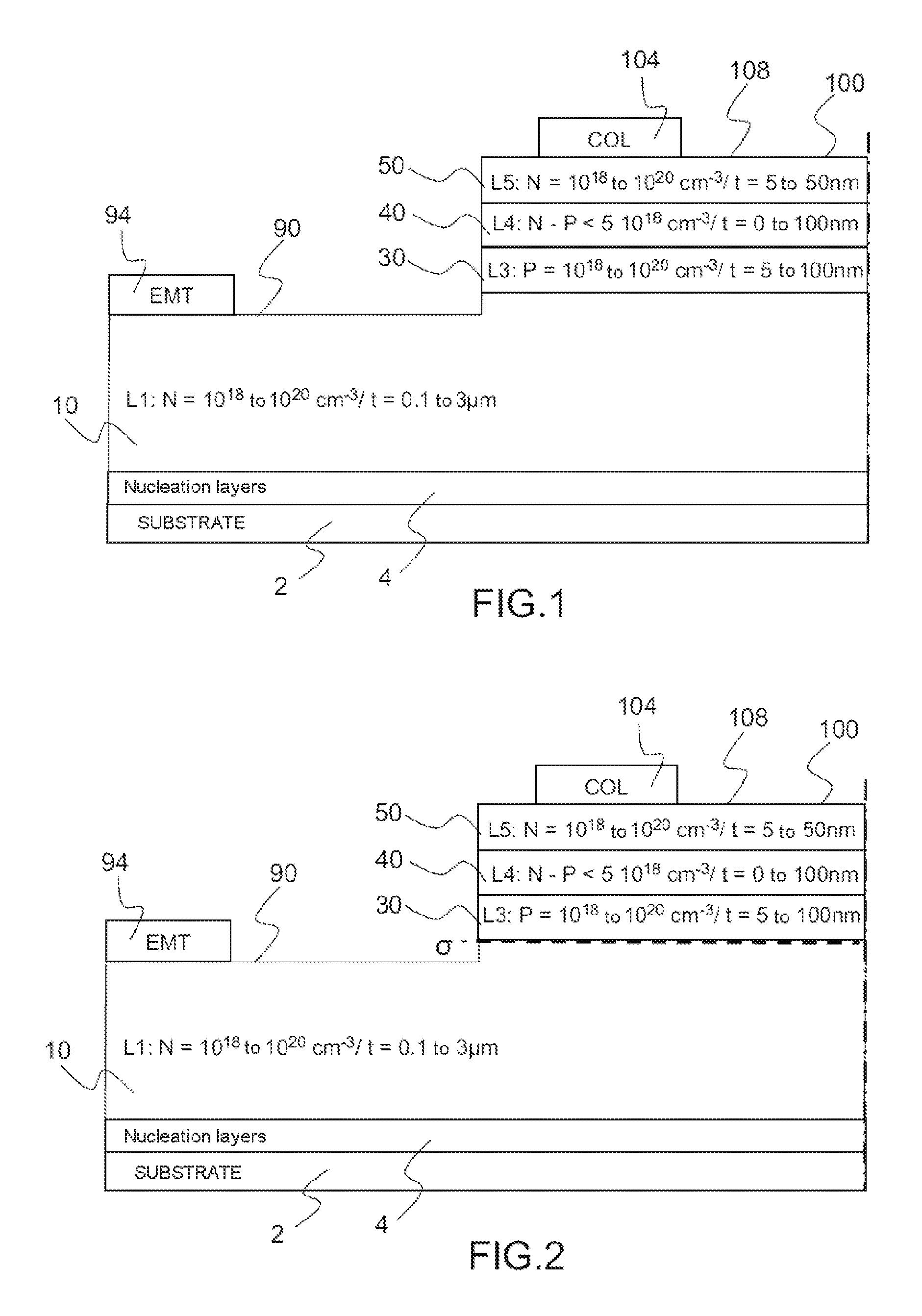
[0063]FIG. 1 shows a cross-sectional view of the electron emission device according to the invention.

[0064]In this first embodiment, a substrate (2) with nucleation layers (4) comprises a stack of semiconductor layers:[0065]a first layer L1 (10) of N type doped between 1018 cm−3 and 1020 cm−3 and of thickness t between 0.1 μm and 3 μm,[0066]on the first layer L1, a layer L3 (30) of P type doped between 1018 cm−3 and 1020 cm−3 and of thickness between 5 nm and 100 nm,[0067]on the layer L3, a layer L4 (40) having a doping of P or N type less than some 1018 cm−3 and of a thickness t between 0 nm and 100 nm,[0068]an output layer L5 (50) on top of the layer L4 of N type doped between 1018 cm−3 and 1020 cm−3 and of thickness between 5 nm and 50 nm.

[0069]The layers L3, L4 and L5 partially cover the layer L1 so as to leave a free surface (90) on this layer L1 for an emitter ohmic land EMT 94 intended to receive a reference potential, for example the potential of a ground M.

[0070]The output ...

second embodiment

[0072]FIG. 2 shows a cross-sectional view of the electron emission device according to the invention.

[0073]In this second embodiment, comprising the stack of layers L1, L3, L4, L5 of FIG. 1, a negative fixed charge (σ−) is obtained partly by doping of the layer L3 with impurities of acceptor type and partly by piezoelectric effect obtained at the interface between the layers L1 and L3 by a suitable choice of the chemical composition of said layers.

third embodiment

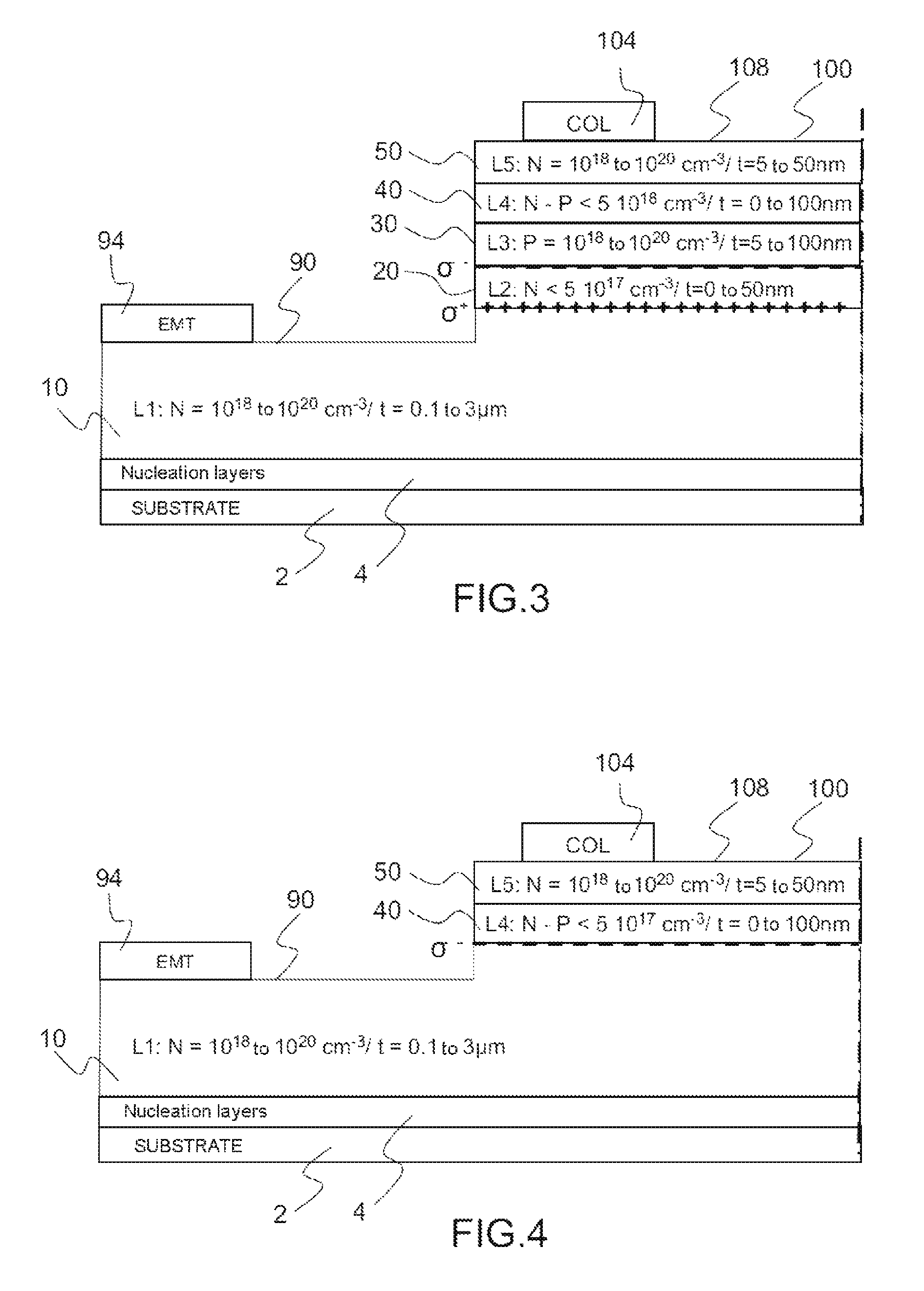
[0074]FIG. 3 shows a cross-sectional view of the electron emission device according to the invention.

[0075]In the embodiment presented in FIG. 3, a layer L2 is added to the stack presented in FIG. 1, having a doping of P or N type less than some 1017 cm−3 and of a thickness t less than 50 nm.

[0076]In this embodiment of FIG. 3, a negative charge σ− is obtained by piezoelectric effect at the interface between the P-doped layer L3 and the layer L2. The layer L2 exhibits a composition difference with the layer L1 such that a positive charge σ+ by piezoelectric effect appears in the interface between the layer L2 and the first layer L1. For example, the different materials of these layers L1 and L2 are chosen from the following chemical compounds:

InyAl1-yN, or AlxGa1-xN, or InxGa1-xN or (InyAl1-y)xGa1-xN


PUM


Abstract

A semiconductor device for electron emission in a vacuum comprises a stack of two or more semi-conductor layers of N and P type according to sequence N / (P) / N forming a juxtaposition of two head-to-tail NP junctions, in materials belonging to the III-N family, two adjacent layers forming an interface. The semiconductor materials of the layers of the stack close to the vacuum, where the electrons reach a high energy, have a band gap Eg>c / 2, where c is the electron affinity of the semiconductor material, the P-type semiconductor layer being obtained partially or completely, by doping impurities of acceptor type or by piezoelectric effect to exhibit a negative fixed charge in any interface between the layers, a positive bias potential applied to the stack supplying, to a fraction of electrons circulating in the stack, the energy needed for emission in the vacuum by an emissive zone of an output layer.

Description

CROSS-REFERENCE TO RELATED APPLICATIONS[0001]This application is a National Stage of International patent application PCT / EP2012 / 064346, filed Jul. 20, 2012, which claims priority to foreign French patent application no. FR 1102286, filed on Jul. 22, 2011.FIELD OF THE INVENTION[0002]The invention relates to the sources of so-called cold electrons using a semiconductor diode.BACKGROUND[0003]Today's electron sources integrated in power microwave amplifier tubes use the thermoelectronic emission obtained by heating electron sources called thermionic cathodes, to temperatures in the vicinity of 1000° C. Because of the physical principle used, these cathodes are limited in terms of emitted electron current and of lifespan, and also include the drawback of taking a fairly long time, of the order of a minute, to obtain the stabilized emission of electrons when they are heated, or switched on.[0004]To circumvent these limitations and improve the efficiency of electron tubes with thermionic ...

Claims


Application Information

Patent Timeline
Patent Type & Authority Patents(United States)
IPC IPC(8): H01J1/308H01J23/04
CPCH01J1/308H01J23/04
Inventor JACQUET, JEAN-CLAUDEAUBRY, RAPHAELPOISSON, MARIE-ANTOINETTEDELAGE, SYLVAIN
Owner THALES SA
Why Eureka
Try Eureka