System and method for cryogenic hybrid technology computing and memory

a hybrid technology and computing system technology, applied in computing models, instruments, magnetic measurements, etc., can solve the problems of long n-bit delay, inconvenient small voltage 200 v for an energy-efficient power supply, and slow down the processor to an unacceptable degree, so as to achieve effective low-loss microstrip transmission lines, easy power dissipation, and easy combination

Active Publication Date: 2018-02-06
SEEQC INC
View PDF105 Cites 9 Cited by
  • Summary
  • Abstract
  • Description
  • Claims
  • Application Information

AI Technical Summary

Benefits of technology

[0023]The modular nature of this preferred architecture has a number of advantages which simplify scaling to larger systems. From a design perspective, the scaling of the processor can proceed from a word size as small as 1 bit, and any problems related to system scale such as global timing, performance margins, and fabrication yield will manifest themselves incrementally, so that they can be isolated and solved efficiently. The register file is similarly modular, making it possible to integrate the processor with the register file in an efficient manner, starting at a word size of two bits. This enables the skewed word high-speed wave-pipelined datapath initiated in the ALU to continue unimpeded into the register file (see FIG. 1), which requires coupling across many DC isolation steps associated with the serial DC biasing.
[0026]In a preferred embodiment of the technology, the circuit comprises at least two distinct wiring layers, one with low inductance and another with high inductance. The high-inductance wiring layer may exhibit substantially enhanced values of inductance based on the property known in the art as kinetic inductance, whereby most of the effective inductance is associated not with magnetic fields external to the conductor (corresponding to conventional magnetic inductance), but rather with kinetic energy of the current-carrying electrons inside the conductor. The kinetic inductance does not couple magnetic fields, but is otherwise equivalent to circuit inductance (V=L dI / dt) for most other purposes. See, for example, U.S. Pat. No. 4,028,714, expressly incorporated herein by reference; also see en.wikipedia.org / wiki / Kinetic_inductance; Chen et al., “Kinetic Inductance Memory Cell”, IEEE Trans. Appl. Supercond., vol. 2, p. 95 (1992); Johnson et al., “Anomalous current dependence of kinetic inductance of ultrathin NbN meander lines”, IEEE Trans. Appl. Supercond., vol. 7, p, 3492 (1997). Any superconducting inductor will comprise both magnetic inductance and kinetic inductance; however, most superconducting inductors in the prior art, particularly those associated with RSFQ circuits, were comprised predominantly of magnetic inductance. In contrast, the high-inductance wiring layer of a preferred embodiment may exhibit an inductance which is comprised predominantly of kinetic inductance. Such an inductor is not constrained by the conventional magnetic relation L˜μ0a, and can have a large inductance in a very small length, enabling increased device density in integrated circuits. Furthermore, the use of inductors dominated by kinetic inductance may reduce the negative effects of parasitic inductive coupling between signals on different connecting lines and with trapped flux.
[0029]A further advantage of a high-inductance layer is that it can be used to restrict propagation of ps pulses on DC bias lines. In RSFQ circuits, a superconducting ground plane is used for shielding of electrical and magnetic signals from different parts of the circuit. In this case, all superconducting interconnects and bias lines are effectively low-loss microstrip transmission lines. Such passive transmission lines are used for transporting signals between different parts of the circuit at high speeds, but bias lines used for DC power distribution should not propagate these signals. In conventional RSFQ circuits, resistors can be inserted to block such pulses, but they will also dissipate power. In energy-efficient RSFQ circuits, such resistors are avoided. Instead, one can insert a short section of an inductive line with a sharply different characteristic impedance for ps pulses, which creates a mismatch that restricts pulse propagation. Such a mismatch can be easily designed using a short length of a high-inductance layer of the present technology.

Problems solved by technology

However, this would require a long N-bit delay for the carry bit to propagate from the Least Significant Bit (LSB) to the Most Significant Bit (MSB).
Even for the ultrafast clock rates fc1 of RSFQ circuits that approach or exceed 100 GHz, a fully synchronous delay period of N / fc1 would slow down the processor to an unacceptable degree.
Such a small voltage ˜200 μV is inconveniently small for an energy-efficient power supply.

Method used


Image

  • System and method for cryogenic hybrid technology computing and memory
  • System and method for cryogenic hybrid technology computing and memory
  • System and method for cryogenic hybrid technology computing and memory

Examples


Embodiment Construction

[0095]I. Superconducting Energy-Efficient Wave-Pipelined Digital Processor

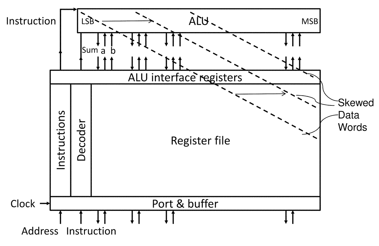
[0096]FIG. 1 shows a conceptual diagram of the wave-pipelined datapath and timing scheme for a proposed high-speed energy-efficient superconducting microprocessor, comprising an arithmetic logic unit (ALU) and register file, with skewed words that represent asynchronous propagation of carry bits through the processor. This multibit ALU comprises a cascade of 1-bit ALUs, and one of its unique features is that both the instruction and the carry bit cascade asynchronously through the ALU. This architecture combines the timing advantage and modular scaling found in a ripple adder with the speed advantage of asynchronous circuitry.

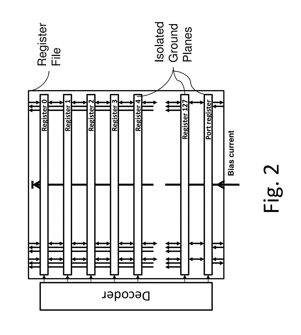
[0097]A block diagram of the architecture of the register file is shown in FIG. 2. This consists of an array of 128 registers, each with an identical modular structure, designed for a 64-bit word. Since the bias current for each of these is the same, this enables the current bias for each...


PUM

PropertyMeasurementUnit
cryogenic temperaturesaaaaaaaaaa
temperatureaaaaaaaaaa
clock frequencyaaaaaaaaaa

Abstract

A system and method for high-speed, low-power cryogenic computing are presented, comprising ultrafast energy-efficient RSFQ superconducting computing circuits, and hybrid magnetic / superconducting memory arrays and interface circuits, operating together in the same cryogenic environment. An arithmetic logic unit and register file with an ultrafast asynchronous wave-pipelined datapath is also provided. The superconducting circuits may comprise inductive elements fabricated using both a high-inductance layer and a low-inductance layer. The memory cells may comprise superconducting tunnel junctions that incorporate magnetic layers. Alternatively, the memory cells may comprise superconducting spin transfer magnetic devices (such as orthogonal spin transfer and spin-Hall effect devices). Together, these technologies may enable the production of an advanced superconducting computer that operates at clock speeds up to 100 GHz.

Description

CROSS REFERENCE TO RELATED APPLICATION[0001]The present application is a Continuation of U.S. patent application Ser. No. 14 / 643,078, filed Mar. 10, 2015, now U.S. Pat. No. 9,520,180, issued Dec. 13, 2016, which claims benefit of priority from U.S. Provisional Patent Application 61 / 951,169, filed Mar. 11, 2014, the entirety of which are expressly incorporated herein by reference.BACKGROUND OF THE INVENTION[0002]The explosive growth of the Internet has transformed data centers into large industrial-scale computer facilities with extraordinarily high energy demands. From Google and Facebook to banking, cloud computing and supercomputing, an average data center already uses as much electricity as a medium-size town. In Silicon Valley, data centers are also listed as the top air polluters from backup diesel exhausts. Already by 2012, the energy costs for a data center were estimated to exceed the cost of the original capital investment over its useful life. The carbon footprint of data ...

Claims


Application Information

Patent Timeline
Patent Type & Authority Patents(United States)
IPC IPC(8): G11C11/44G11C11/16
CPCG11C11/44G11C11/161G11C11/1673G11C11/1653G11C7/1006G11C7/1075G11C2207/007G01R33/0354G01R33/1284G11C11/18G11C11/1675G06N10/00A61K8/0212A61K8/20A61K8/25A61K8/345A61K8/42A61K8/733A61Q19/00A61Q19/08H10N69/00H10N60/12
Inventor MUKHANOV, OLEG A.KIRICHENKO, ALEXANDER F.VERNIK, IGO V.NEVIRKOVETS, IVAN P.KADIN, ALAN M.
Owner SEEQC INC
Why Eureka
Try Eureka