

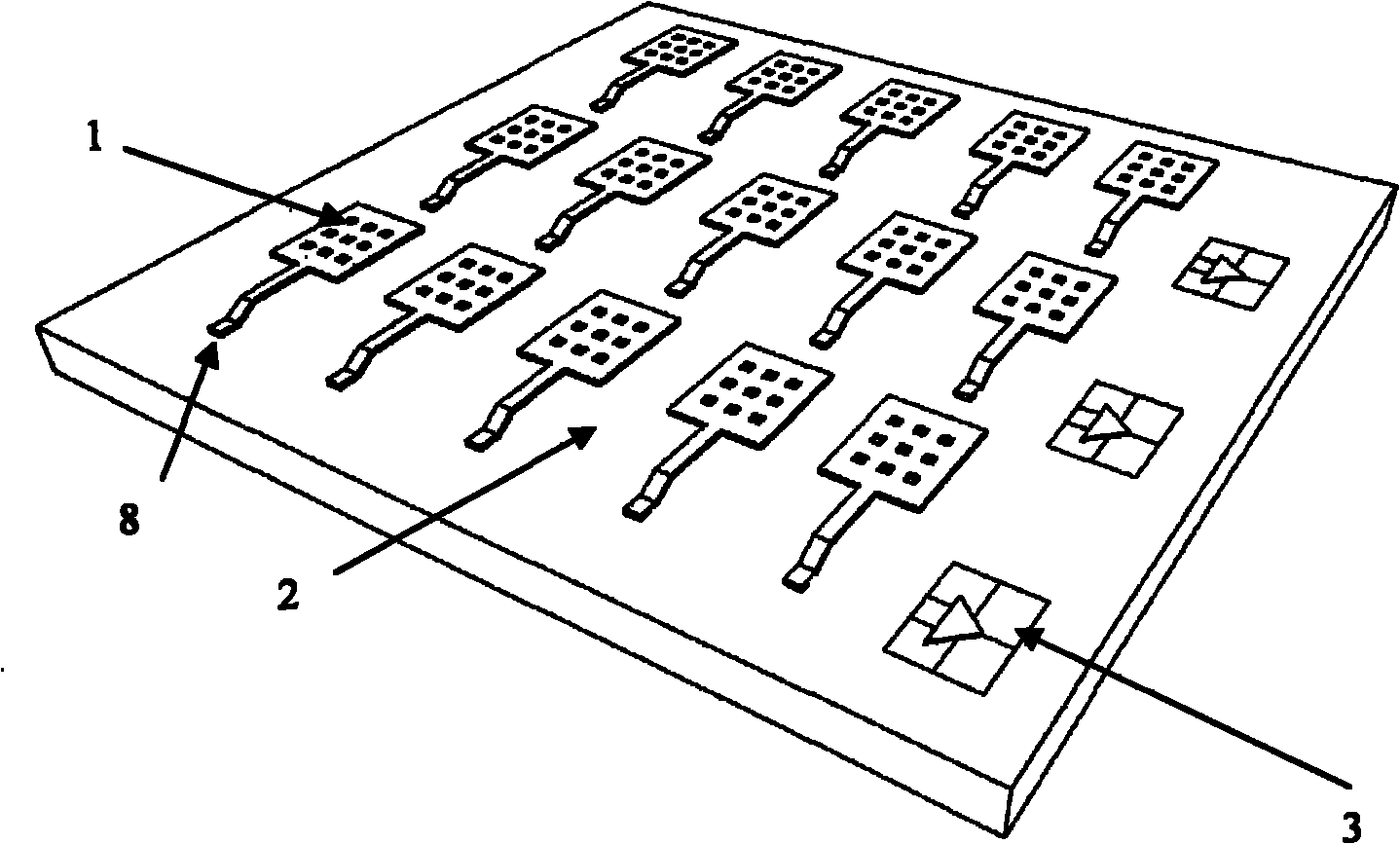
Non-refrigerating infrared focal plane array as well as preparation method and application thereof
A focal plane array and uncooled infrared technology, which is applied in the field of infrared and thermal sensing, can solve the problems of poor system shock resistance, difficulty in machine integration, and bulky optical readout system
- Summary
- Abstract
- Description
- Claims
- Application Information
AI Technical Summary
Problems solved by technology
Method used
Image

Examples
Embodiment 1
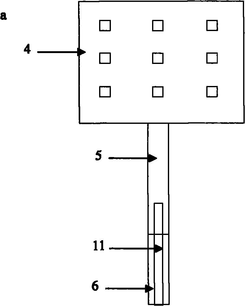
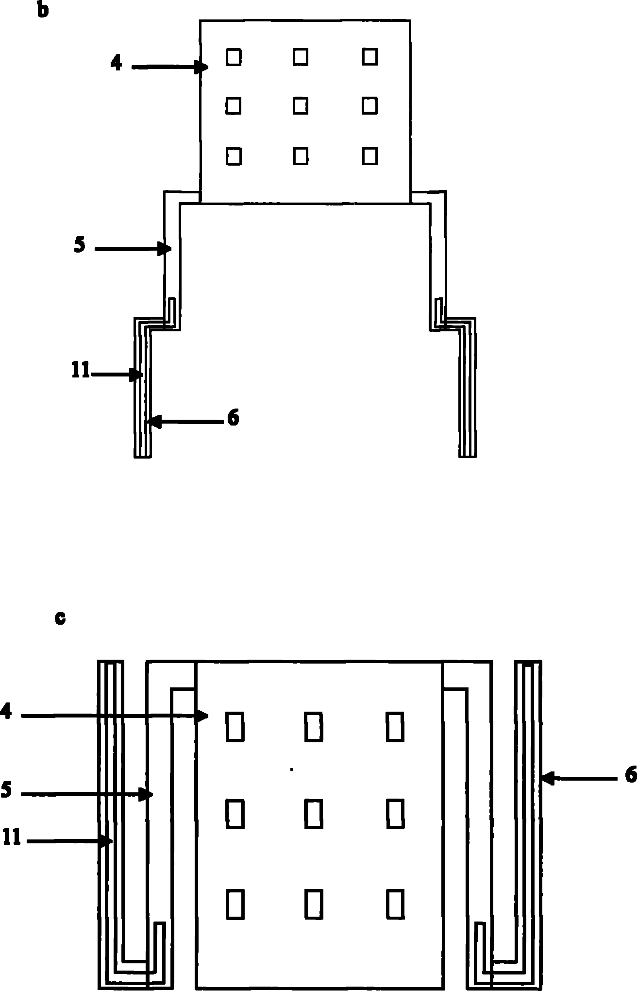
[0067] Figure 7 The flow chart for the preparation of a MOSFET readout micro-cantilever infrared focal plane array, the specific steps are as follows:
[0068] 1) Adopt SOI silicon wafer 1 as processing substrate, device layer 2 is P-type, device layer 2 thickness is 200nm, (100) crystal orientation, buried oxide layer 3 thickness is 400nm ( Figure 7 a); first, 30nm silicon device layer is oxidized to provide a stress buffer layer for the subsequent process; a layer of SiNx is LPCVD on the surface of the SOI silicon wafer, with a thickness of 100nm, and the first photolithography is performed, and the SiNx is dry etched, and the photolithography is removed Glue to form the active region 4 of the MOSFET device;
[0069] 2) Oxidize the Si device layer to form silicon islands 4 in the active area electrically insulated from each other; carry out the second photolithography, implant boron ions in the active area, the implantation voltage is 40keV, and the dose is 2×10 12 / cm ...
Embodiment 2
[0078] Follow the steps below to prepare a MOSFET readout uncooled infrared focal plane array:
[0079] 1) Using SOI silicon wafer 1 as the processing substrate, the device layer 2 is N-type, the thickness of the device layer 2 is 400nm, (100) crystal orientation, and the thickness of the buried oxide layer 3 is 1 μm ( Figure 7 a); first carry out 50nm silicon device layer oxidation; LPCVD a layer of SiNx on the surface of the SOI silicon wafer with a thickness of 100nm, perform photolithography for the first time, dry etch SiNx, and remove the photoresist;
[0080] 2) Oxidize the Si device layer to form silicon islands 4 in the active area electrically insulated from each other; carry out the second photolithography, implant boron ions in the active area, the implantation voltage is 40keV, and the dose is 1×10 11 / cm 2 , form the P-region 5, remove the photoresist; carry out the third photolithography, inject phosphorus, the implantation voltage is 60kev, and the implantati...
PUM
| Property | Measurement | Unit |
|---|---|---|
| Thermal expansion coefficient | aaaaa | aaaaa |
| Thermal expansion coefficient | aaaaa | aaaaa |
| Thermal conductivity | aaaaa | aaaaa |
Abstract
Description
Claims
Application Information