Substrate processing apparatus and substrate processing method

a processing apparatus and substrate technology, applied in the direction of instruments, photosensitive materials, furnaces, etc., can solve the problems of reducing the durability and reliability affecting the processing efficiency and limiting the speed of the main handler operation, so as to suppress the generation of particles and increase the throughput

Inactive Publication Date: 2001-12-18
TOKYO ELECTRON LTD
View PDF15 Cites 20 Cited by
  • Summary
  • Abstract
  • Description
  • Claims
  • Application Information

AI Technical Summary

Benefits of technology

It is an object of the present invention to provide a substrate processing apparatus and a substrate processing method in which a substrate can be conveyed...

Problems solved by technology

However, since the 4-axis drive operations in the X-axis direction, Y-axis direction, Z-axis direction, and .theta.-rotation-axis direction are independently performed in the conventional main handler, the speed of the main handler operation is limited to a certain speed.
Therefore, a time from when the main handler reaches a target point to when the main handler receive a wafer is too long so that it is very difficult to increase the throughput.
In addition, when each drive system employs a high-speed drive mechanism to more increase the operation of the main handler, an excessive load acts on the mechanism, its durabi...

Method used


Image

  • Substrate processing apparatus and substrate processing method
  • Substrate processing apparatus and substrate processing method
  • Substrate processing apparatus and substrate processing method

Examples


first embodiment

A main handler according to the present invention will be described below with reference to FIGS. 5 to 10.

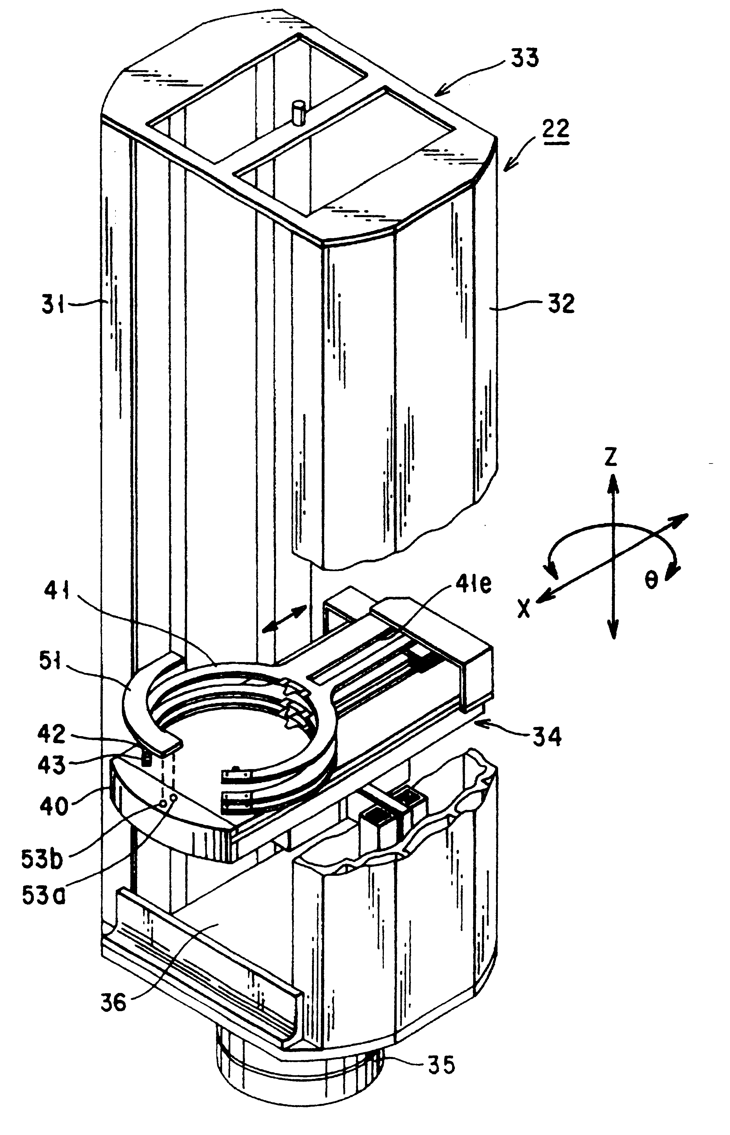
The casing of the main handler 22 is constituted by a cylindrical support member 33, and an arm section 34 is arranged in the cylindrical support member 33 such that the arm section 34 can be vertically moved in the Z-axis direction. The cylindrical support member 33 comprises a pair of vertical wall portions 31 and 32 which are connected to each other at the upper and lower ends and opposite to each other.

As shown in FIG. 6, the cylindrical support member 33 is connected to the vertical drive shaft of a motor 35. When the cylindrical support member 33 is rotated about the vertical drive shaft, the arm section 34 is rotated together with the cylindrical support member 33, thereby rotating the arm section 34 about the Z axis at an angle .theta.. Note that the cylindrical support member 33 may be constituted to be connected to another rotating shaft (not shown) rotated by the moto...

second embodiment

the present invention will be described below with reference to FIGS. 14 to 18E. The same reference numerals as in the first embodiment denote the same parts in the second embodiment, and a description thereof will be omitted.

In an apparatus according to the second embodiment, an acceleration acting on a main handler 222 is controlled depending on the moving distance to a target point. In addition, the wafer contact / holding portion of a third holding arm 241 consists of a material having a high friction coefficient to cope with control of the acceleration of the main handler 222.

An arm section 34 of the main handler 222 comprises a first holding arm 243, a second holding arm 242, and the third holding arm 241 which are sequentially arranged from below. Of these holding arms, the lower two holding arms 243 and 242 are the same as those of the first embodiment.

The third holding arm 241 at the uppermost portion, as shown in FIGS. 16 and 17, comprises a holding member 241a having a flat...


PUM


Abstract

A wafer processing apparatus includes a common path, extending in a Y-axis direction, in which one wafer or a plurality of wafers are conveyed, a plurality of process units stacked on both sides of the common path to constitute multi-stage structures, a main handler moved in the common path in the Y-axis direction and rotated about a Z axis at an angle theta to load/unload the wafer into/from the process units, an arm section arranged to move in the main handler in the Z-axis direction, a plurality of holding arms arranged in the arm section to constitute a multi-stage structure so as to respectively hold the wafers, each holding arm being advanced and retreated on an X-Y plane from the arm section, an optical sensor, arranged in the arm section, for detecting a holding state of the wafer in each of the plurality of holding arms, and a controller for controlling an operation of the main handler, an operation of the arm section, and operations of the plurality of holding arms on the basis of a detection result from the optical sensor, wherein the controller advances or retreats each holding arm while operating at least one of the main handler and the arm section, and causes the optical sensor to detect the holding state of the wafer by each holding arm before the holding arm reaches a corresponding one of the process units.

Description

BACKGROUND OF THE INVENTION1. Field of the InventionThe present invention relates to substrate processing apparatus and a substrate processing apparatus for processing a substrate such as a semiconductor wafer.2. Description of the Related ArtIn a photolithography process in manufacturing a semiconductor device, a resist coating process for coating a resist on a wafer and a developing process for developing a coated resist after an exposure process. These processes are simultaneously performed by using a composite process system described in, e.g., U.S. Pat. No. 5,339,128. This system comprises a main handler for conveying a wafer, and is designed such that a wafer W is loaded by the main handler from a cassette station into a process section, the wafer W are exchanged between process chambers in the process section, and the above processes are performed.A conventional handler has an arm section driven by three axes (Y axis, Z axis, and .theta. rotation axis), and the arm section a ...

Claims


Application Information

Patent Timeline
IPC IPC(8): H01L21/67H01L21/687H01L21/677B65G49/07H01L21/00
CPCH01L21/6715H01L21/67781H01L21/68707H01L21/68
Inventor OHKURA, JUNIIDA, NARUAKIKUDOU, HIROYUKITATEYAMA, MASANORISAKAMOTO, YASUHIRO
Owner TOKYO ELECTRON LTD
Why Eureka
Try Eureka