

Data processor and method of processing data
- Summary
- Abstract
- Description
- Claims
- Application Information
AI Technical Summary
Benefits of technology
Problems solved by technology
Method used
Image

Examples
first preferred embodiment
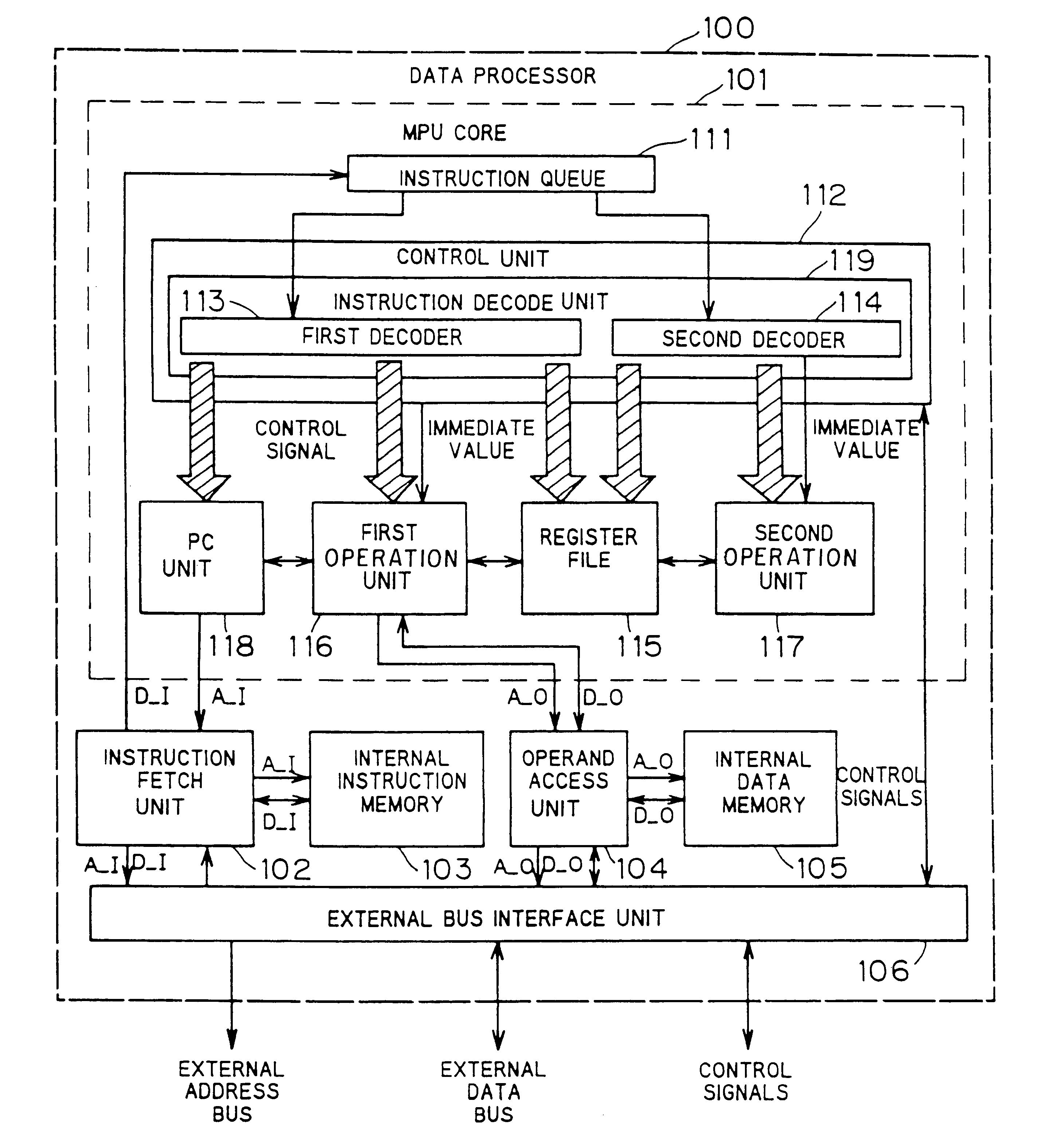
A data processor according to a first preferred embodiment of the present invention will be described below. The data processor of the first preferred embodiment is a 16-bit processor whose addresses and data are 16 bits in length.
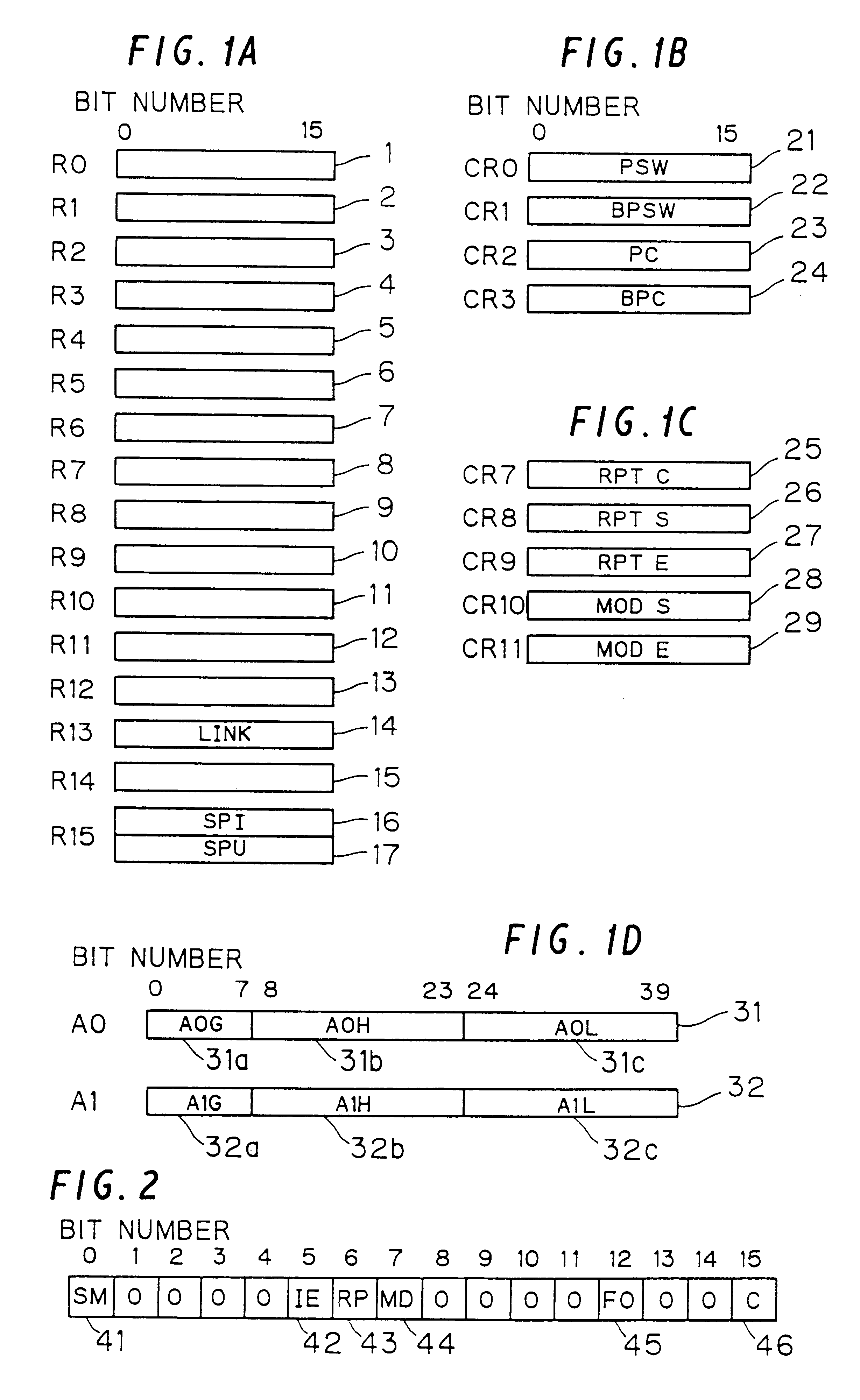
FIG. 1 illustrates a set of registers for the data processor of this preferred embodiment. The data processor employs big endian bit and byte ordering wherein the most significant bit is the bit 0.
Sixteen general-purpose registers R0 to R15 are provided for storing data and address values therein. The general-purpose registers R0 to R14 are designated by the numerals 1 to 15 in FIG. 1, respectively. The general-purpose register R13 (designated at 14 in FIG. 1) is allocated as a link (LINK) register for storing a return address for a subroutine jump. The general-purpose register R15 is a register for a stack pointer (SP) including an interruption stack pointer (SPI) 16 and a user stack pointer (SPU) 17. A processor status word (PSW) to be described later sw...
second preferred embodiment
FIG. 28 is a block diagram of a second operation unit 120 for the data processor according to a second preferred embodiment of the present invention corresponding to the second operation unit 117 of the first preferred embodiment. Other units of the data processor of the second preferred embodiment are similar in construction to those of the first preferred embodiment. The second operation unit 120 differs from the second operation unit 117 of the first preferred embodiment in that it includes an ALU 221 operable independently of an adder 231 for performing the multiply-add operation. This allows the execution of the addition and subtraction of the multiply-add / multiply-subtract instructions and other arithmetic and logic operations without interference of hardware.
The ALU 221 performs a 16-bit arithmetic and logic operation. An A2 latch 222 connected to the S4 bus 304 and a B2 latch 223 connected to the S5 bus 305 are input latches for the ALU 221. An ALUO latch 225 is an output la...
third preferred embodiment
FIG. 35 is a functional block diagram of the data processor according to a third preferred embodiment of the present invention. An MPU 850 is an MPU core. An instruction fetch unit 863 and an operand access unit 864 are substantially similar to the instruction fetch unit 102 and operand access unit 104 of the data processor of the first preferred embodiment. The instruction data which are 64 bits in length are applied to the instruction fetch unit 863. The bus interface unit and the like are not shown in FIG. 35.
The MPU core 850 comprises an instruction queue 851, a control unit 852, a register file 860, a first operation unit 858, a second operation unit 859, a third operation unit 861, and a fourth operation unit 862. The instruction queue 851 is an FIFO-controlled instruction buffer for holding a maximum of two 64-bit instructions. The first operation unit 858 includes an incrementor, a decrementor, and an adder and performs management of the PC value, calculation of the branch t...
PUM
 Abstract
Description
Claims
Application Information