Method for producing light-emitting device

一种发光装置、制造方法的技术,应用在化学仪器和方法、半导体/固态器件制造、气态化学镀覆等方向,能够解决降低放射强度、易劣化等问题

Inactive Publication Date: 2008-11-26
SHIN-ETSU HANDOTAI CO LTD
View PDF5 Cites 2 Cited by
  • Summary
  • Abstract
  • Description
  • Claims
  • Application Information

AI Technical Summary

Problems solved by technology

MgZnO-type oxides can be formed by the above-mentioned MOVPE process or MBE process, but the formation process is likely to be the reason for the lack of oxygen in MgZnO-type oxides, and it is easy to deteriorate the crystallinity of the ZnO-containing active layer, thus extending the reason for this active layer. The total half-value width of the emission wavelength range of the source layer, which reduces the emission intensity and suppresses the desired emission efficiency of a specific wavelength

Method used


Image

  • Method for producing light-emitting device
  • Method for producing light-emitting device
  • Method for producing light-emitting device

Examples


Embodiment 3

[0091] Figure 13 Is a schematic diagram showing an example of a specific light-emitting device in Embodiment 3 of the present invention;

[0092] Figure 14A Is description Figure 13 Diagram of an example manufacturing process of a light-emitting device;

[0093] Figure 14B Yes to continue Figure 14A Diagram of processing steps;

[0094] Figure 14C Yes to continue Figure 14B Diagram of processing steps;

[0095] Figure 15 It is a schematic diagram of corundum crystal structure;

[0096] Figure 16A Is a schematic diagram illustrating the operation of the method for manufacturing a light-emitting device according to the third embodiment of the present invention;

[0097] Figure 16B Is description Figure 16A Diagram of subsequent operations;

[0098] Figure 16C Is description Figure 16B Diagram of subsequent operations;

[0099] Figure 16D Is description Figure 16C Diagram of subsequent operations;

[0100] Figure 17 is an example Figure 14A~14C The diagram of...

Embodiment 1

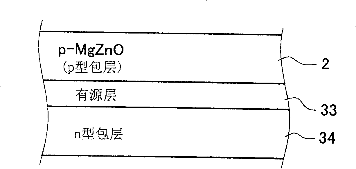
[0113] figure 1 The stacking structure of an important part of the light-emitting device of the first invention is schematically shown. The device has a light-emitting layer portion in which an n-type cladding layer 34, an active layer 33, and a p-type cladding layer 2 are sequentially stacked. P-type cladding 2 is composed of p-type Mg x Zn 1-x O layer (0≤x≤1): sometimes referred to as p-type MgZnO layer 2 hereinafter. In the p-type MgZnO layer 2, a trace amount of one, two or more of N, Ga, Al, In, and Li is included as p-type dopants: as described above, the p-type carrier concentration is adjusted to 1×10 16 ~8×10 18 Place / cm 3 Within the range, especially 10 17 ~10 18 Place / cm 3 Within the range of the left and right.

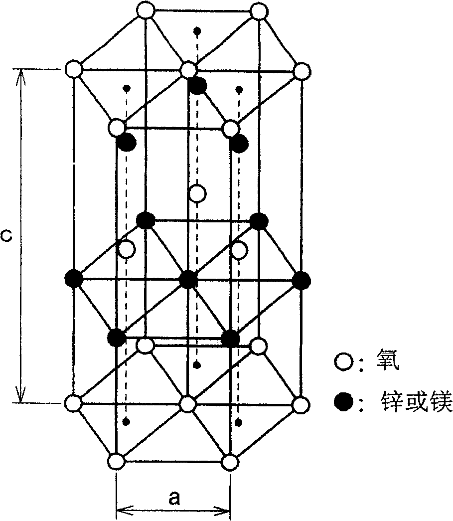
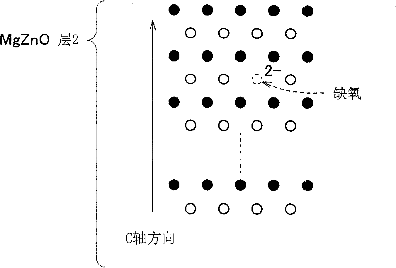
[0114] figure 2 It is a schematic diagram of the crystal structure of MgZnO, showing the so-called Wurtzite structure. In this structure, the oxygen ion filling plane and the metal ion (Zn or Mg ion) filling plane are alternately stacked along the c-axis d...

Embodiment 2

[0163] An embodiment of the second invention will be described below. Because the basic part of the light-emitting device to which the second invention is applied is the same as that described in Embodiment 1, it will not be described in detail (see figure 1 ~4 and Figures 10A and 10B). Such as Figure 6 As shown in (a), the GaN buffer layer 11 is still epitaxially grown on the sapphire substrate 10, and then a p-type MgZnO layer 52 (typically 50nm thick), MgZnO active layer 53 (typically 30nm thick) and n Type MgZnO layer 54 (generally 50 nm thick) (the reverse is also possible). The epitaxial growth of each layer in this example can be performed by the MOVPE process similar to that described in Embodiment 1, but there are several differences as follows. More specifically, when the MgZnO active layer 53 and the p-type MgZnO layer 52 are grown here, an ultraviolet lamp (such as an excimer ultraviolet lamp) as an ultraviolet light source is provided on the main surface of the oppo...


PUM

PropertyMeasurementUnit
band gapaaaaaaaaaa
band gapaaaaaaaaaa
wavelengthaaaaaaaaaa

Abstract

In a first invention, a p-type MgxZn1-xO-type layer is grown based on a metal organic vapor-phase epitaxy process by supplying organometallic gases which serves as a metal source, an oxygen component source gas and a p-type dopant gas into a reaction vessel. During and / or after completion of the growth of the p-type MgxZn1-xO-type layer, the MgxZn1-xO-type thereof is annealed in an oxygen-containing atmosphere. This is successful in forming the layer of p-type oxide in a highly reproducible and stable manner for use in light emitting device having the layer of p-type oxide of Zn and Mg. In a second invention, a semiconductor layer which composes the light emitting layer portion is grown by introducing source gases in a reaction vessel having the substrate housed therein, and by depositing a semiconductor material produced by chemical reactions of the source gas on the main surface of the substrate. A vapor-phase epitaxy process of the semiconductor layer is proceed while irradiating ultraviolet light to the main surface of the substrate and the source gases. This is successful in sharply enhancing reaction efficiency of the source gases when the semiconductor layer for composing the light emitting layer portion is formed by a vapor-phase epitaxy process, and in readily obtaining the semiconductor layer having only a less amount of crystal defects. In a third invention, a buffer layer having at least an MgaZn1-aO-type oxide layer on the contact side with the light emitting layer portion is grown on the substrate, and the light emitting layer portion is grown on the buffer layer. The buffer layer is oriented so as to align the c-axis thereof to the thickness-wise direction, and is obtained by forming a metal monoatomic layer on the substrate based on the atomic layer epitaxy, and then by growing residual oxygen atom layers and the metal atom layers. This is successful in obtaining the light emitting portion with an excellent quality. In a fourth invention, a ZnO-base semiconductor active layer included in a double heterostructured, light emitting layer portion is formed using a ZnO-base semiconductor mainly composed of ZnO containing Se or Te, so as to introduce Se or Te, the elements in the same Group with oxygen, into oxygen deficiency sites in the ZnO crystal possibly produced during the formation process of the active layer, to thereby improve crystallinity of the active layer. Introduction of Se or Te shifts the emission wavelength obtainable from the active layer towards longer wavelength regions as compared with the active layer composed of ZnO having a band gap energy causative of shorter wavelength light than blue light. This is contributive to realization of blue-light emitting devices.

Description

Technical field [0001] The present invention relates to a light emitting device and a manufacturing method thereof. Background technique [0002] There has long been a demand for high-brightness light-emitting devices that can generate short-wave radiation in the blue light region. Such light-emitting devices have recently been implemented using AlGaInN-based materials. By combining this device with red and green high-brightness light-emitting devices, rapid progress has also been made in applying it to full-color light-emitting devices or display devices. However, the application of AlGaInN-based materials will inevitably increase the cost, because the material contains the main elements Ga and In, both of which are relatively rare metals. One of the other main problems of this material is that its growth temperature is as high as 700~1000℃, and it consumes considerable energy during production. This is not only undesirable in terms of cost reduction, but also does not want to g...

Claims


Application Information

Patent Timeline
Patent Type & Authority Patents(China)
IPC IPC(8): H01L33/00H01L21/365C23C16/30C23C16/40C30B25/02C30B25/10C30B25/18
CPCH01L21/365H01L21/02554H01L21/02472H01L21/02507H01L21/0242H01L33/0083C30B25/02C30B25/105C30B25/183H01L21/02483C23C16/40H01L21/0262H01L21/02477H01L21/02579H01L21/02565H01L21/0248C30B29/16
Inventor 石崎顺也
Owner SHIN-ETSU HANDOTAI CO LTD
Why Eureka
Try Eureka