Minute pattern photoetching method

A lithography pattern and micro technology, which is applied to microlithography exposure equipment, photolithography process exposure devices, electrical components, etc., can solve the problems of high price, high cost, and increase the complexity of the production process, so as to improve production capacity and simplify the production process. The effect of mass production process and cost reduction

Inactive Publication Date: 2008-12-31
SEMICON MFG INT (SHANGHAI) CORP +1
View PDF4 Cites 0 Cited by
  • Summary
  • Abstract
  • Description
  • Claims
  • Application Information

AI Technical Summary

Problems solved by technology

However, since the exposure equipment used for lithography is expensive, these methods are costly and will increase the complexity of the production process to varying degrees.

Method used


Image

  • Minute pattern photoetching method
  • Minute pattern photoetching method
  • Minute pattern photoetching method

Examples


Embodiment Construction

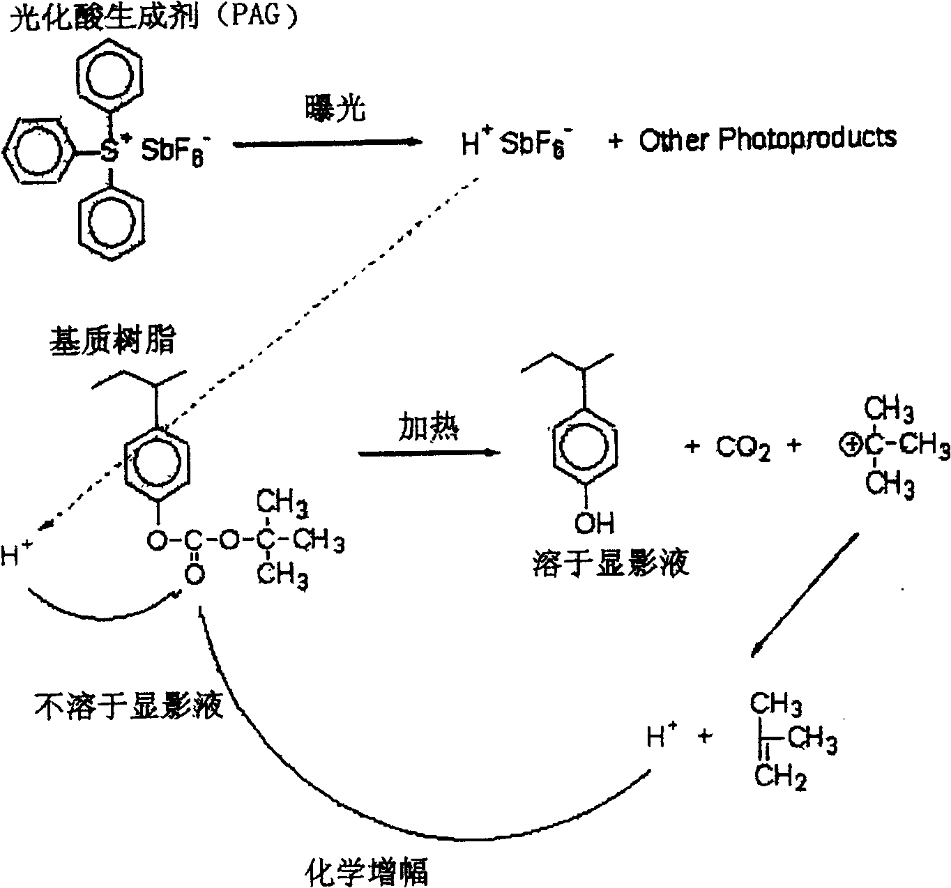
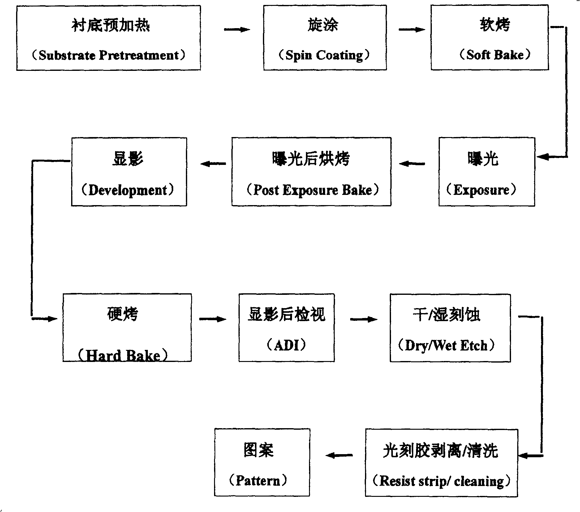
[0032] The invention provides a method for fine photolithographic patterns, which mainly includes coating a layer of bottom layer resin on the entire etched substrate layer surface; coating a layer of photoresist on the upper surface of the bottom layer resin layer; The layer is exposed to the required pattern, and baked after exposure; the photoresist layer and the underlying resin layer are developed in the developer, and a photoresist pattern is formed on the photoresist and the underlying resin layer; the photoresist and the underlying resin layer are used as the etching The etch stop layer is selectively etched to transfer the pattern onto the substrate.

[0033] According to the method of the present invention, the substrate material can be any thin film material that is etched or ion-implanted to transfer a pattern or form a desired pattern in a specific area, which is generally used in semiconductor manufacturing such as DRAM.

[0034] According to the present inventio...


PUM

PropertyMeasurementUnit
thicknessaaaaaaaaaa

Abstract

A microlithographic patterning method using an improved deep ultraviolet (DUV) photoresist and underlying resin. This method can reduce the thickness of the photoresist without using the optical improvement method, and realize the safe aspect ratio of the lithography pattern, thereby improving the resolution of the pattern and the uniformity of the critical dimension, the exposure latitude and the depth of focus. Due to the use of the underlying resin, the hard mask required by the usual thin-layer photoresist is not required in the subsequent etching process, and a high-resolution transfer pattern on the substrate is obtained, so that the application of DUV photoresist can be extended to 0.11μm and the following techniques. The application of this method can simplify the mass production process, reduce the cost and increase the production capacity.

Description

technical field [0001] The present invention relates to a microlithographic patterning method, in particular to a method for microlithographic patterning using Deep UltraViolet photoresist (Photoresist) (hereinafter referred to as DUV photoresist) and underlying resin. Background technique [0002] Lithography is one of the most important steps in the production process of semiconductor devices such as VLSI. The pattern (pattern) and doping (doping) area of ​​each layer of film related to the structure of the MOS element are determined by photolithography. [0003] In lithography, the photosensitive material photoresist is applied on the semiconductor wafer substrate, and the photoresist is irradiated through a specific photomask, because the photomask has patterns, and these patterns reflect the incident light from the light source , so that the light beam that is not reflected and passes through the photomask also has the same pattern as the photomask, and the photoresist...

Claims


Application Information

Patent Timeline
Patent Type & Authority Patents(China)
IPC IPC(8): G03F7/20H01L21/027
Inventor 崔彰日
Owner SEMICON MFG INT (SHANGHAI) CORP
Why Eureka
Try Eureka