Compound and organic electroluminescent element using the same
A technology of electroluminescent components and compounds, applied in the direction of electroluminescent light sources, electrical components, electric light sources, etc., can solve problems such as insufficient satisfaction, and achieve the effects of increasing current value, high efficiency, and high solubility
- Summary
- Abstract
- Description
- Claims
- Application Information
AI Technical Summary
Problems solved by technology
Method used
Image
Examples
Embodiment 1
[0122]
[0123]
[0124] 1g (1.35mmol) of compound A, 672mg (3.39mmol) of 2-biphenylboronic acid, 156mg of Pd (PPh 3 ) 4 , 20ml of toluene, 10ml of ethanol, and 20ml of 2M aqueous sodium carbonate solution were added to a 100ml round bottom flask, and then the whole mixture was stirred at 80°C for 8 hours in a nitrogen stream. After the reaction was completed, the formed product was extracted with toluene, and the organic layer was dried over magnesium sulfate. After this time, the drying agent was filtered off and the solvent was distilled off. The residue was dissolved in chloroform, and the solution was separated and purified by alumina column chromatography, followed by recrystallization from toluene. The formed crystals were vacuum-dried at 120° C., and the formed product was subjected to sublimation and purification to obtain 700 mg of Exemplified Compound No. X-25 (58% yield).
[0125] The M+ of 882.4 as the compound was confirmed using matrix assisted laser des...
Embodiment 2
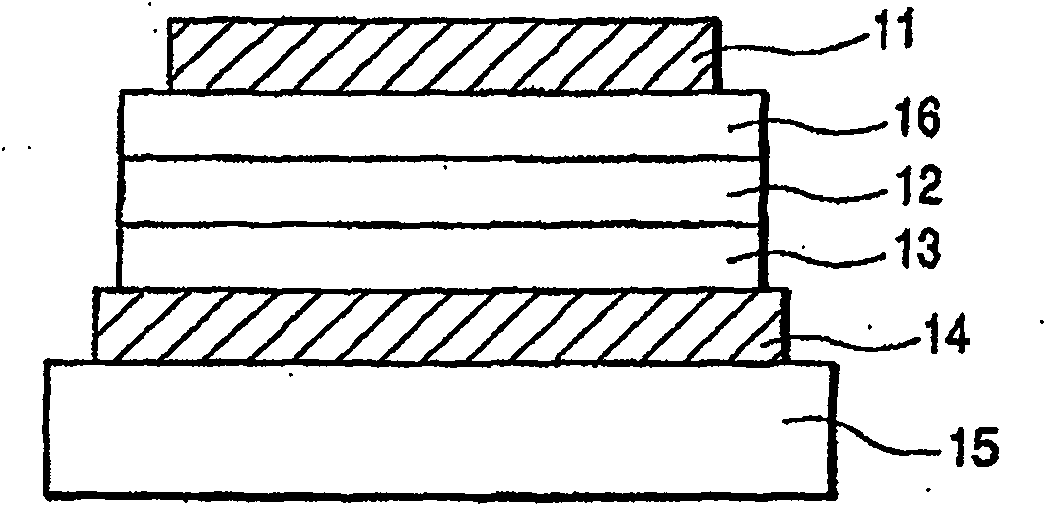
[0130] In this example, in Figure 1B A device with three organic layers shown in was used as the device structure.
[0131] ITO (as transparent electrode 14 ) having a thickness of 100 nm was patterned on a glass substrate (as transparent substrate 15 ). Utilized in a 10 -5 The following organic layers and electrode layers were successively formed on the ITO substrate by the vacuum evaporation method of resistance heating in a vacuum chamber at a pressure of Pa so that the opposing electrode area was 3mm 2 .
[0132] Hole transport layer 13 (50nm): α-NPD
[0133] Emitting layer 12 (50nm): [host] example compound No.X-25, [guest] Ir (4mopiq) 3 (weight ratio: 4%) and Ir(bq) 3 (weight ratio: 8%)
[0134] Electron transport layer 16 (50 nm): Bphen (manufactured by DOJINDO LABORATORIES) Metal electrode layer 1 (1 nm): KF
[0135] Metal electrode layer 2 (130nm): Al
[0136] The current-voltage characteristic of the EL element was measured by using a microammeter 4140B (man...
Embodiment 3
[0150]
[0151]
[0152] 2g (3.13mmol) of compound B, 1.38g (6.89mmol) of 2-bromophenylboronic acid, 400mg of Pd (PPh 3 ) 4 , 20 ml of toluene, 10 ml of ethanol, and 20 ml of 2M aqueous sodium carbonate solution were added to a 100 ml round bottom flask, and then the whole mixture was stirred at 80° C. for 4 hours under nitrogen flow. After the reaction was completed, the formed product was extracted with toluene, and the organic layer was dried over magnesium sulfate. After this time, the drying agent was filtered off and the solvent was distilled off. The residue was dissolved in chloroform, and the solution was separated and purified using silica gel chromatography, followed by recrystallization from toluene, thereby obtaining 1.37 g of Compound C (63% yield).
[0153] 694.1 as M+ of the compound was observed using matrix-assisted laser desorption / ionization-time-of-flight mass spectrometry (MALDI-TOF MS).
[0154] In addition, the structure of the compound was conf...
PUM
| Property | Measurement | Unit |
|---|---|---|
| thickness | aaaaa | aaaaa |
| glass transition temperature | aaaaa | aaaaa |
| glass transition temperature | aaaaa | aaaaa |
Abstract
Description
Claims
Application Information


