

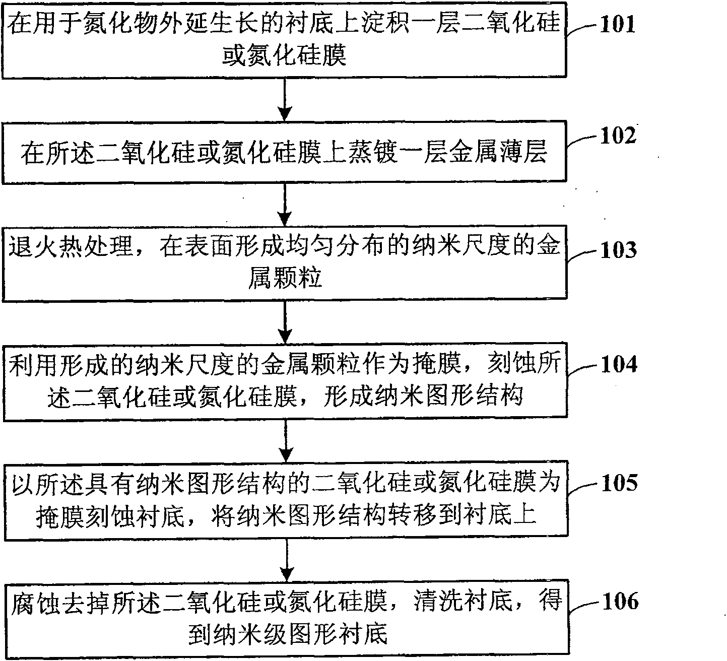
Method for preparing nano-scale pattern substrate for nitride epitaxial growth
A technology of epitaxial growth and graphic substrate, which is applied in the manufacture of semiconductor/solid-state devices, electrical components, circuits, etc., can solve the problems of expensive equipment, incapable of large-scale production, high cost, etc., so as to reduce production costs and realize The effect of scale and large-area production
- Summary
- Abstract
- Description
- Claims
- Application Information
AI Technical Summary
Problems solved by technology
Method used
Image

Examples
Embodiment 1
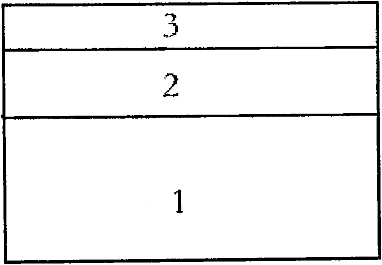
[0052] This embodiment is a method for fabricating a nanoscale patterned sapphire substrate for nitride epitaxial growth. Sapphire substrate is one of the most commonly used substrate materials for epitaxial nitride growth.
[0053] First, a 0.5-micron silicon dioxide film is deposited on a 2-inch sapphire substrate by plasma-enhanced chemical vapor deposition (PECVD), and then a 15-nm nickel metal layer is evaporated by electron beam evaporation. The structure profile is as follows: figure 2 shown;
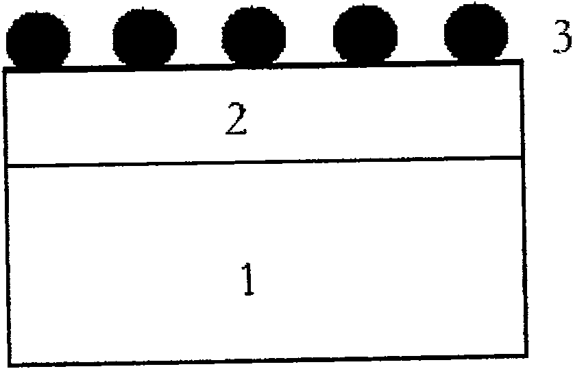
[0054] Then, under flowing N2, anneal at a temperature of 850 degrees for 5 minutes, so that nano-scale nickel metal particles are formed on the surface, and the structural section is as follows image 3 shown;
[0055] Then use nano-scale nickel metal particles as a mask, and use RIE or ICP plasma etching equipment to dry-etch the silicon dioxide film to form a nano-pattern structure. The scale of the pattern is about 50-150nm, and the structure profile is Figure 4 shown; ...
Embodiment 2
[0059] This embodiment is a method for fabricating a nanoscale patterned Si(111) substrate for nitride epitaxial growth. Si(111) substrate is one of the commonly used substrate materials for epitaxial nitride growth.
[0060] First, a 0.5 micron silicon nitride film is deposited on a Si(111) substrate by PECVD technology and a 15nm titanium (Ti) metal thin layer is evaporated by electron beam method. The structure profile is as follows: figure 2 shown;
[0061] Then in the flowing N 2 Annealing at 950°C for 20 minutes to form nanoscale titanium (Ti) metal particles with a structural profile such as image 3 shown;
[0062] Then use nanometer-scale metal titanium (Ti) particles as a mask, and use RIE or ICP equipment to dry-etch the silicon nitride film to form a nano-graphic structure. The graphic scale is about 100-300nm, and the structural section is as follows Figure 4 shown;
[0063] Then use the silicon nitride film of the nano-pattern structure as a mask, and use ...
PUM
| Property | Measurement | Unit |
|---|---|---|
| thickness | aaaaa | aaaaa |
| thickness | aaaaa | aaaaa |
| thickness | aaaaa | aaaaa |
Abstract
Description
Claims
Application Information