Sample enrichment chip, manufacturing method and enrichment method and on micronano structure
What is AI technical title?
AI technical title is built by Patsnap AI team. It summarizes the technical point description of the patent document.
A micro-nano structure and enrichment technology, applied in the field of analytical chemistry, to achieve the effects of portability, small size and simple operation
Inactive Publication Date: 2007-07-18
SHANGHAI INST OF MICROSYSTEM & INFORMATION TECH CHINESE ACAD OF SCI
View PDF0 Cites 16 Cited by
Summary
Abstract
Description
Claims
Application Information
AI Technical Summary
This helps you quickly interpret patents by identifying the three key elements:
Problems solved by technology
Method used
Benefits of technology
Problems solved by technology
There are few reports on this
Method used
Image
Click on the blue label to locate the original text in one second.
Reading with bidirectional positioning of images and text.
Examples
Embodiment 1
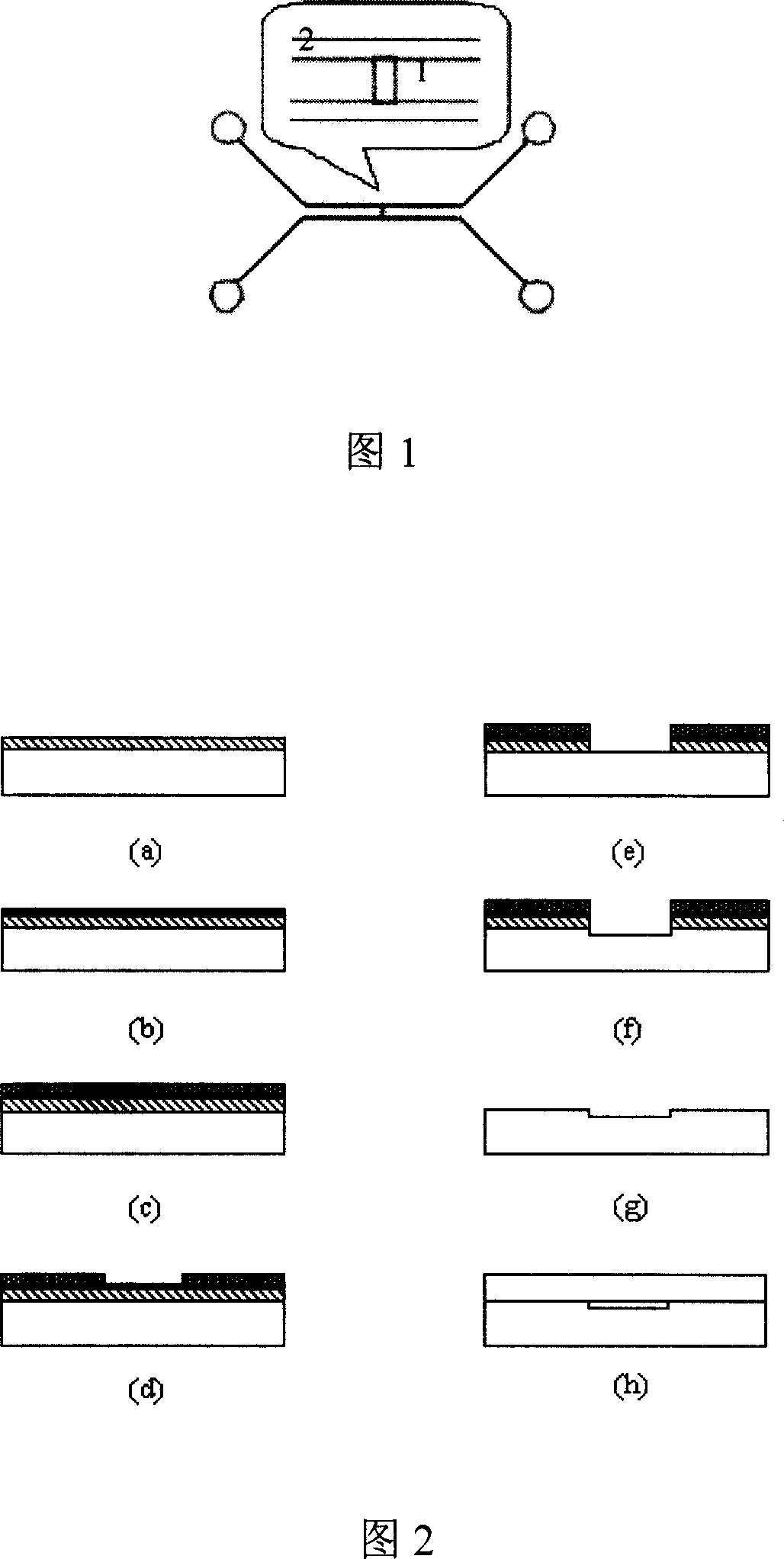
[0023] Example 1 Manufacturing process of sample enrichment chip based on micro-nano structure
[0024] 1. First, nano-channels and nano-scale transmission pipes are processed on the surface of quartz glass by MEMS technology
[0025] A. Fabrication of micron-scale transmission pipes
[0027] ①Cleaning: ultrasonically clean the quartz glass substrate with acetone, ethanol, and deionized water for 5 minutes; blow dry with nitrogen; dry,
[0028] ② Evaporate hexamethyldisiloxane, apply photoresist 6809 and spin the glue, the speed is 4000rpm, the glue throwing time is 30s,
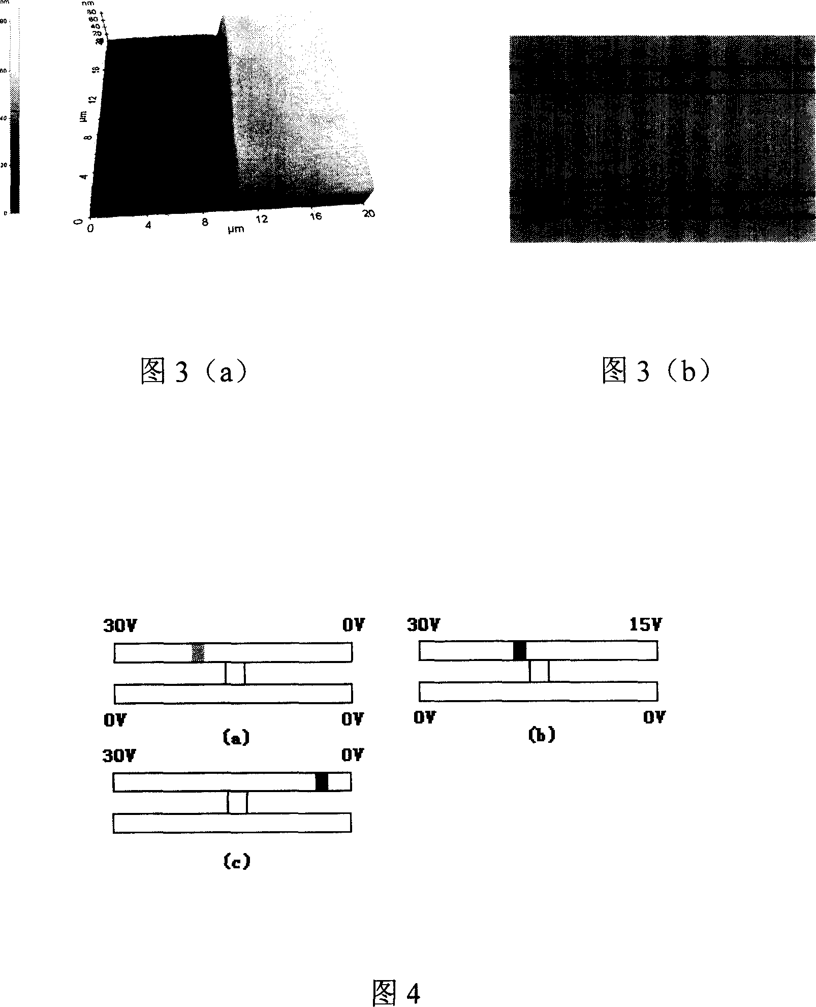
[0060] The enrichment method of embodiment 2 enrichment chip
[0061] On the basis of the chip after low-temperature bonding in Example 1, the following two process steps are used to achieve enrichment
[0062] 1. Chip surface treatment: use 1mol / L NaOH solution to fill the newly bonded chip, rinse 3 times, let stand for 30min, and rinse with deionized water.
[0063] 2. The protein labeled with FITC fluorescent dye is used as the sample, and 0.75mmol / L boric acid is used as the buffer solution; the sample is transferred to the nano-ion trap area with a 30V DC voltage, as shown in Figure 4 (a); the sample band is due to The ions caused by the nanometer region are trapped, piled up and enriched continuously, as shown in Figure 4(b); the compressed sample is tuned by using voltage, and introduced into the detection area for sample detection, as shown in Figure 4(c).
PUM
Property
Measurement
Unit
depth
aaaaa
aaaaa
Abstract
The invention relates to sample enrichment chip, manufacturing method and enrichment method based on micro nanostructure. Its feature is that the enrichment chip is used quartz glass as backing material, formed by enrichment nanometer channel and micro sample transmitting pipeline. It applies MEMS technique to process the channel and pipeline one the quartz glass, strictly control channel depth to make it satisfy ion falling demand, utilizes low temperature bonding method to process for the substrate and covering piece, fills sample into chip pipeline, adds direct voltage in the sample pool to form electric field in nanometer channel. Because of Debyelayers in the channel are superposed, while ion falling zoon is formed beside the channel. The sample moved under the action of the electric field is enriched beside the channel to form sample enrichment zoon. The chip has small volume, will not destroy enrichment component while enriching.
Description
technical field [0001] The present invention relates to a highly efficient sample enrichment chip based on micro-nano structure and its manufacturing method, more precisely to a sample enrichment chip based on micro-nano structure, its manufacturing method and its sample enrichment method based on the principle of iontrapping. It belongs to the field of analytical chemistry. Background technique [0002] Micro total analysis system (also known as lab-on-a-chip) is a concept proposed by Manz et al in the 1990s. The basic operation units such as sample preparation, biological and chemical reactions, separation, and detection are fully integrated or partially integrated on a chip of several square centimeters to complete different biological or chemical reaction processes and analyze their products. After more than ten years of development, the separation, analysis and detection systems of nucleic acids, proteins, organic compounds and inorganic ions on microchips have develo...
Claims
Application Information
Patent Timeline
Application Date:The date an application was filed.
Publication Date:The date a patent or application was officially published.
First Publication Date:The earliest publication date of a patent with the same application number.
Issue Date:Publication date of the patent grant document.
PCT Entry Date:The Entry date of PCT National Phase.
Estimated Expiry Date:The statutory expiry date of a patent right according to the Patent Law, and it is the longest term of protection that the patent right can achieve without the termination of the patent right due to other reasons(Term extension factor has been taken into account ).
Invalid Date:Actual expiry date is based on effective date or publication date of legal transaction data of invalid patent.
Patent Type & AuthorityApplications(China)
IPC IPC(8): G01N1/34G01N30/08
Inventor金庆辉刘菁赵建龙
OwnerSHANGHAI INST OF MICROSYSTEM & INFORMATION TECH CHINESE ACAD OF SCI

