Non polarity A side nitride film growing on the silicon(102) substrate and its making method and use

A non-polar, nitride technology, applied in the field of non-polar A-side nitride thin film

Inactive Publication Date: 2007-08-01
INST OF PHYSICS - CHINESE ACAD OF SCI
View PDF0 Cites 121 Cited by
  • Summary
  • Abstract
  • Description
  • Claims
  • Application Information

AI Technical Summary

Problems solved by technology

[0007] The purpose of the present invention is to overcome the existing polarity problem in the GaN-based material (InGaAlN) that grows on the (0001) plane, while existing substrates (R plane sapphire and LiAlO 3 (100) plane) the problem of high defects in growing non-polar GaN-based thin films

Method used


Image

  • Non polarity A side nitride film growing on the silicon(102) substrate and its making method and use
  • Non polarity A side nitride film growing on the silicon(102) substrate and its making method and use

Examples


Embodiment 1

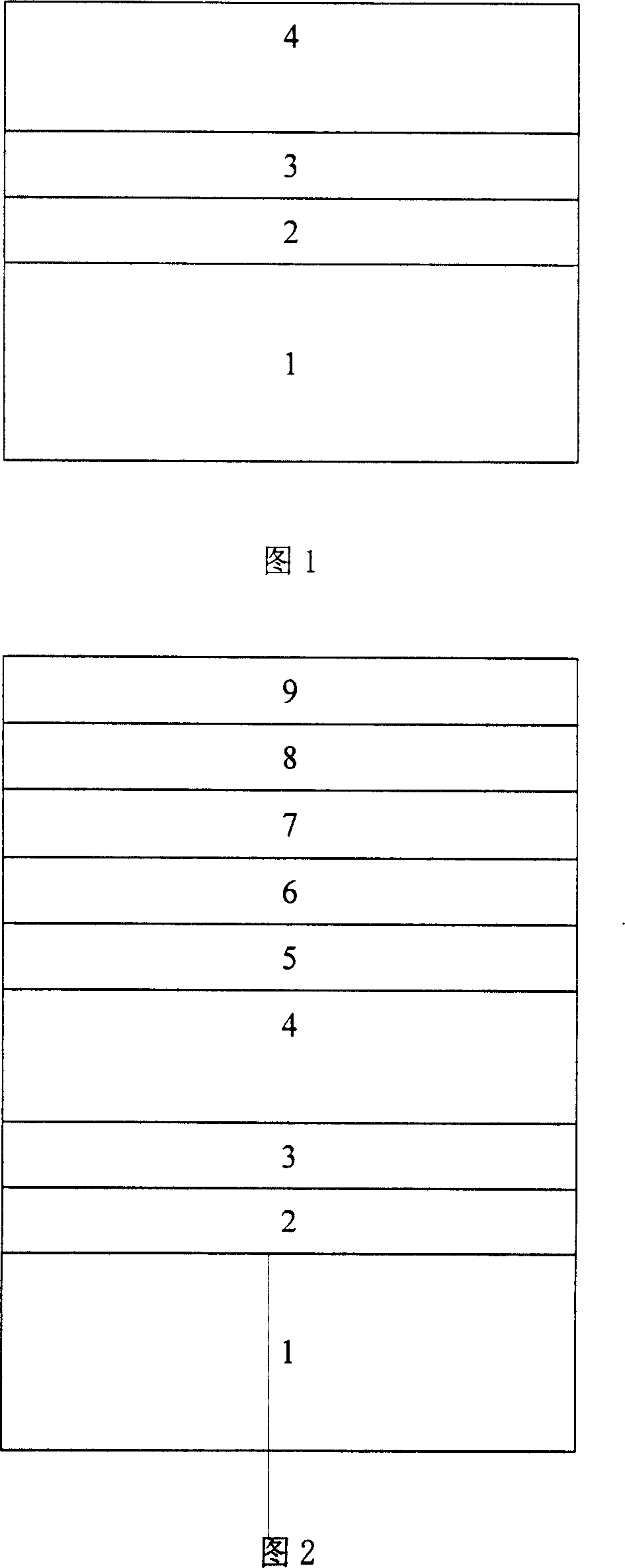
[0059] Embodiment 1, preparation of the non-polar A-side nitride thin film grown on the silicon substrate

[0060] A substrate with an off-angle of 5 degrees from silicon (102) to (010) is used, the thickness of the silicon wafer is 300 microns, the silicon wafer is N-type doped, and has low resistivity. After the silicon wafer is treated with organic solvent and hydrofluoric acid, it is sent into the MOCVD reaction chamber. The temperature of the reaction chamber is raised to 1100° C., the atmosphere of the reaction chamber is hydrogen, and the surface of the cleaned silicon substrate is annealed for desorption treatment to remove the oxide layer on the surface of the substrate. The temperature of the reaction chamber was lowered to 450°C, hydrogen was used as the carrier gas, and trimethylaluminum was passed through, and an Al metal layer with a thickness of 10 angstroms was deposited and grown on the surface of the silicon substrate through the pyrolysis reaction of trimeth...

Embodiment 2

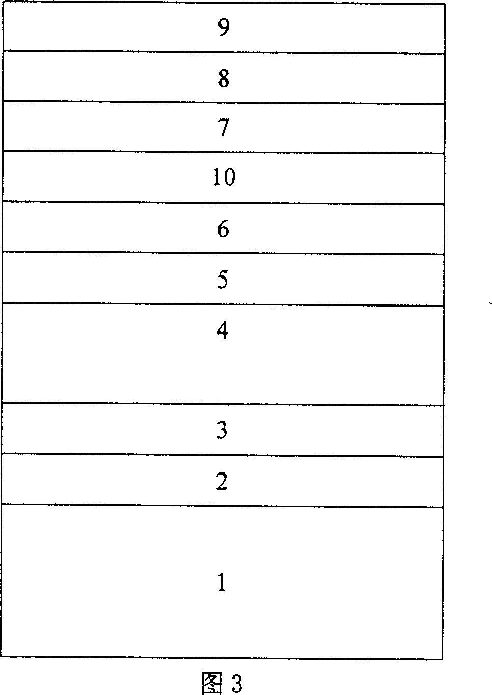
[0061] Embodiment 2, preparation of the non-polar A-side nitride thin film grown on the silicon substrate

[0062] Using a pattern substrate with an off-angle of 12 degrees from silicon (102) to (010), the pattern on the surface of the silicon wafer is a one-dimensional grating pattern with a width of 6 microns, a height of 2 microns, and a pitch of 6 microns, prepared by dry etching , the thickness of the silicon wafer is 300 microns, the silicon wafer is N-type doped, and has low resistivity. After the silicon wafer is treated with organic solvent and hydrofluoric acid, it is sent into the MOCVD reaction chamber. The temperature of the reaction chamber is raised to 600° C., the atmosphere of the reaction chamber is hydrogen, and the surface of the cleaned silicon substrate is annealed for desorption treatment to remove the oxide layer on the surface of the substrate. The temperature of the reaction chamber is lowered to 400°C, hydrogen is used as the carrier gas, and trimet...

Embodiment 3

[0063] Embodiment 3, preparation of the non-polar A-side nitride thin film grown on the silicon substrate

[0064]A silicon (102) substrate is used, the thickness of the silicon wafer is 300 microns, the silicon wafer is N-type doped, and has low resistivity. After the silicon wafer is treated with organic solvent and hydrofluoric acid, it is sent into the MOCVD reaction chamber. The temperature of the reaction chamber is raised to 600° C., the atmosphere of the reaction chamber is hydrogen, and the surface of the cleaned silicon substrate is annealed for desorption treatment to remove the oxide layer on the surface of the substrate. The temperature of the reaction chamber is lowered to 400°C, and the initial growth layer of InGaAlN is directly grown. With hydrogen as the carrier gas, trimethylaluminum and ammonia gas are passed through, and through the reaction of the two, the growth thickness of 100 angstroms AlN layer; the reaction chamber is heated to 600°C, and the AlN l...


PUM

PropertyMeasurementUnit
thicknessaaaaaaaaaa
thicknessaaaaaaaaaa
thicknessaaaaaaaaaa

Abstract

The invention relates to a nonpolar A side nitride film that comprises a silicon (102) underlay, metal layer which grows upon the silicon underlay sequentially, InGaAlN initial growth layer and the first InGaAlN buffer layer, it characterized in that: said silicon underlay is Si underlay which adopts the (102) side or offset angle. The nonpolar a side nitride film which grows on the silicon underlay can be used in LBD, laser, solar battery. The component extension configuration is adopted according to different component, for example the LBD and laser, and using the mature silicon craft further to produce relative diprosopia electrode component or peeling off component. The advantages of the invention are: the invention can increase the growth quality of nonpolar GaN base material, and decrease the cost; the craft of current component can be simplified greatly, the cost can be decreased, and increase the elimination efficiency and lightening efficiency greatly.

Description

technical field [0001] The invention relates to a non-polar A-face nitride thin film grown on a silicon (102) substrate, a preparation method thereof, and an application in optoelectronic and microelectronic devices. Background technique [0002] The wide bandgap material represented by GaN is the third generation semiconductor after Si and GaAs. Due to breakthroughs in epitaxy technology, there was rapid development during the nineties. The reason why it has been widely and highly valued is based on three reasons: first, it is made into a high-brightness blue light-emitting tube, so that human beings can obtain a high-repeatability, long-life panchromatic light source including white light; the second is that it can be made Compared with long-wave lasers, short-wavelength lasers have a small beam spot size, which can realize high-density data optical storage; the third is its high temperature resistance, high thermal conductivity, and high pressure resistance, which can de...

Claims


Application Information

Patent Timeline
Patent Type & Authority Applications(China)
IPC IPC(8): H01L33/00H01L31/0248H01L31/18H01L21/3205H01L21/20H01S5/00C23C16/44
CPCY02P70/50
Inventor 陈弘贾海强周均铭郭丽伟
Owner INST OF PHYSICS - CHINESE ACAD OF SCI
Why Eureka
Try Eureka