Method for manufacturing grid structure of semiconductor device

A technology of gate structure and manufacturing method, which is applied in the field of gate structure manufacturing of complementary metal oxide semiconductor devices, and can solve problems such as depression of active region and LDD region, etc.

Active Publication Date: 2007-09-19
SEMICON MFG INT (SHANGHAI) CORP +1
View PDF1 Cites 7 Cited by
  • Summary
  • Abstract
  • Description
  • Claims
  • Application Information

AI Technical Summary

Problems solved by technology

[0005] Therefore, the object of the present invention is to provide a method for manufacturing the gate structure of a semiconductor device. When etching the gate oxide layer, the plasma source adopts a pulsed output power mode to etch the gate oxide layer to solve the existing problems. The problem that the plasma penetrates the gate oxide layer and recesses the active area and LDD area below it in the technology

Method used


Image

  • Method for manufacturing grid structure of semiconductor device
  • Method for manufacturing grid structure of semiconductor device
  • Method for manufacturing grid structure of semiconductor device

Examples


Embodiment Construction

[0024] The invention discloses a method for manufacturing a gate structure of a semiconductor device. It has high precision for etching gate oxide layer of 65nm and below. The method can be used to manufacture a semiconductor device with an extremely thin gate oxide layer of an ultra-large-scale integrated circuit (ULSI).

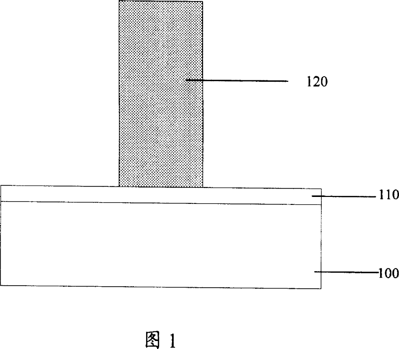
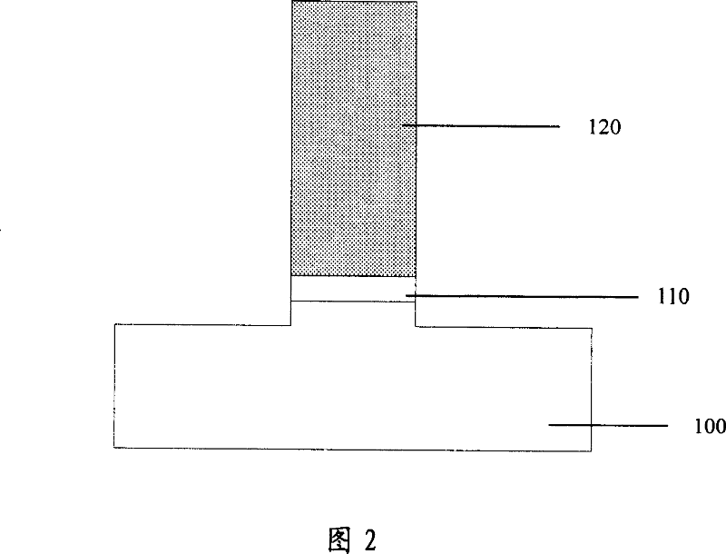
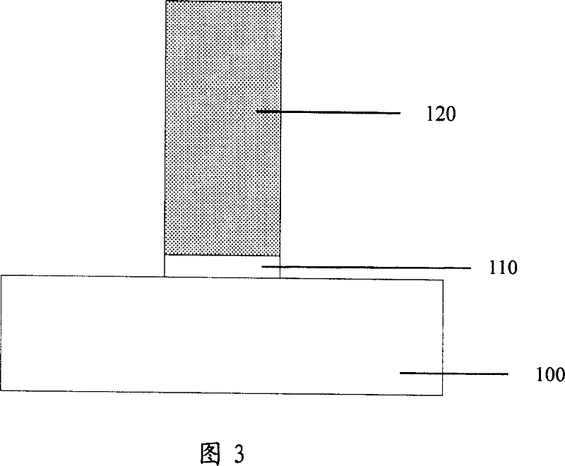
[0025] The present invention also includes a manufacturing method of a field effect transistor, such as a complementary metal oxide semiconductor (CMOS) field effect transistor, which includes a metal gate electrode and an ultra-thin gate dielectric layer (such as 10-20 Ȧ). FIG. 1 is a schematic diagram of a gate structure of a semiconductor device. As shown in FIG. 1 , a gate oxide layer 110 and a gate electrode layer 120 are formed on a substrate 100 . The process flow includes the process done on the thin film layer during the gate fabrication process. The photolithography process and its sub-processes (such as exposure, glue coating, substrate cleani...


PUM


Abstract

The invention provides a mehtod for making grid structure of semiconductor device, which includes providing a semiconductor substrate, and forming a grid medium layer on the substrate, and forming a grid electrode layer on the grid medium layer, and forming a mask layer on the grid electrode layer, and then inducing etching gas to etch the polysilicon grid electrode layer by employing plasma output by a plasma source, wherein the plasma source etches the grid medium layer in pulse outputting power manner. The invention provide method for making grid structure of semiconductor device is very effective for accuracy controlling the thickness of the grid oxide layer in a process node no more then 65 nm, and the etching depth can perfectly stop at the surface of the grid oxide layer without hurting the surface of an active region.

Description

technical field [0001] The invention relates to the technical field of manufacturing semiconductor integrated circuits, in particular to a method for manufacturing a gate structure of a complementary metal oxide semiconductor device. Background technique [0002] With the rapid development of semiconductor manufacturing technology, in order to achieve faster computing speed, larger data storage capacity and more functions of semiconductor devices, semiconductor wafers are developing towards higher component density and high integration. The gate of CMOS devices The poles are getting thinner and shorter than ever. In order to avoid the short channel effect and obtain the maximum drain current, the thickness of the gate oxide layer is usually made thinner and thinner. Using a thinner gate oxide layer can enhance the coupling between the gate electrode and channel carriers, making the characteristics of the transistor closer to that of a long-channel device. Since drain curre...

Claims


Application Information

Patent Timeline
Patent Type & Authority Applications(China)
IPC IPC(8): H01L21/28H01L21/3065H01L21/311H01L21/336
Inventor 吴汉明
Owner SEMICON MFG INT (SHANGHAI) CORP
Why Eureka
Try Eureka