

Metal circuit board of aluminum baseplate magnetic-controlled sputtering-jetted and LED illuminating device
A magnetron sputtering, circuit board technology, applied in the direction of electric solid devices, printed circuit components, circuits, etc., can solve the problems of long production cycle, decreased insulation performance, high energy consumption, etc., achieve good heat dissipation performance, improve heat dissipation Efficiency, the effect of reducing the number of thermal resistances
- Summary
- Abstract
- Description
- Claims
- Application Information
AI Technical Summary
Problems solved by technology
Method used
Image

Examples
Embodiment 1
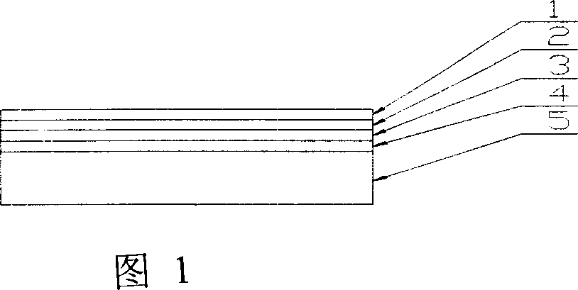
[0046] Embodiment 1: with reference to accompanying drawing 1. A method for manufacturing an aluminum-based insulating oxide magnetron sputtering circuit board, the aluminum plate is subjected to insulating oxidation treatment and an insulating oxide layer is formed, and a mask or photolithography is used to form a circuit pattern on the surface of the insulating oxide layer, and the method of magnetron sputtering is adopted Make the circuit pattern form the metallization layer. The method of magnetron sputtering is a prior art, so it will not be described here. The metallization layer is composed of a base film, a conductive film, and a welding film. ①The base film uses magnetron sputtering metal chromium or titanium to deposit chromium or titanium on the insulating oxide layer. The thickness of the base film is in the range of 0.1 to 0.15 μm. And the control can arbitrarily determine its value within its range, including the end value. ② The conductive film is deposited on...
Embodiment 2
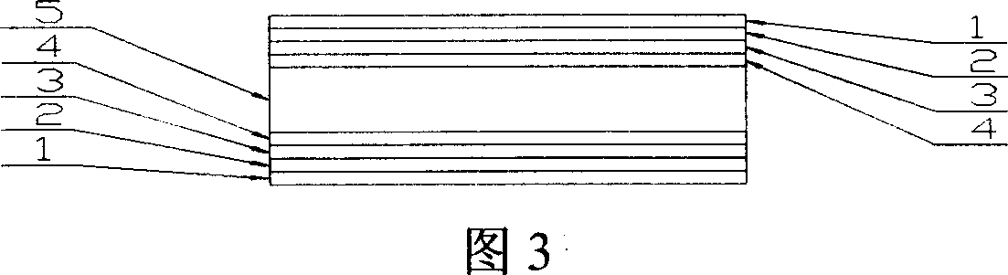
[0047] Embodiment 2: with reference to accompanying drawing 3. On the basis of Example 1, a mask or photolithography method is used to form a circuit pattern on the insulating oxide layer on both sides of the aluminum plate, and the circuit pattern is formed into a metallized layer by magnetron sputtering to form a double-sided aluminum-based circuit board. .
Embodiment 3
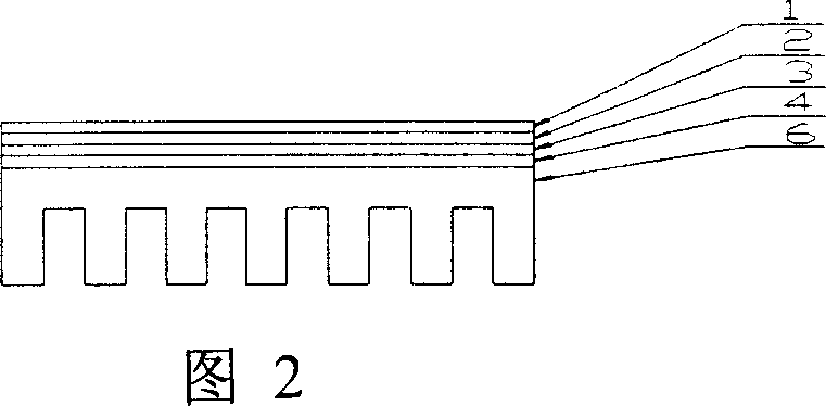
[0048] Embodiment 3: with reference to accompanying drawing 1. A method for encapsulating electronic components on an aluminum-based insulating oxide magnetron sputtering circuit board, which includes an aluminum plate for insulating oxidation treatment and forming an insulating oxide layer, and electronic components, ① using a mask on the mounting surface of the aluminum plate or aluminum radiator film or photolithography to form electronic components packaging circuit patterns, ② using magnetron sputtering method to make the circuit patterns form a metallization layer circuit, ③ electronic components are packaged on the metallization layer circuit, the electronic components are High-power LED tubes, power modules, etc.
PUM
| Property | Measurement | Unit |
|---|---|---|
| Thickness | aaaaa | aaaaa |
| Thickness | aaaaa | aaaaa |
| Thickness | aaaaa | aaaaa |
Abstract
Description
Claims
Application Information