
Eureka
For R&D, Eureka makes reading and utilizing patents & technical documents easy.
Eureka AIR
Designed for self-driven R&D workflows. Generate viable solutions, solve complex R&D challenges, empower your innovation with AI.

Eureka Materials
Designed for material experts only. Revolutionize your material R&D, from search, analyze, to developing new materials.

TechResearch
Generate reliable direction feasibility study reports for your R&D in just a few steps.

TechSeek
Discover and master advanced knowledge NOW. Basics, ideas, possibilities, all at once.

TechMind
As an expert in R&D Theories, TechMind can generates customized viable solutions instantly.

TechRisk
Analyze your overall solution with one click, know your potential R&D risks in advance.

TechMonitor
Get weekly tech updates, stay abreast of the latest tech innovations and key insights.
Near-infrared high-transmission rate non-crystal transparent conductive oxide film and its making method
An oxide thin film, transparent conductive technology, which is applied in the manufacture of oxide conductors, non-metallic conductors, cables/conductors, etc., can solve the problems of reduced electrical conductivity and achieve low resistivity, uniform film, and good process stability.
- Summary
- Abstract
- Description
- Claims
- Application Information
AI Technical Summary
Problems solved by technology
Method used
Image

Examples
Embodiment 1
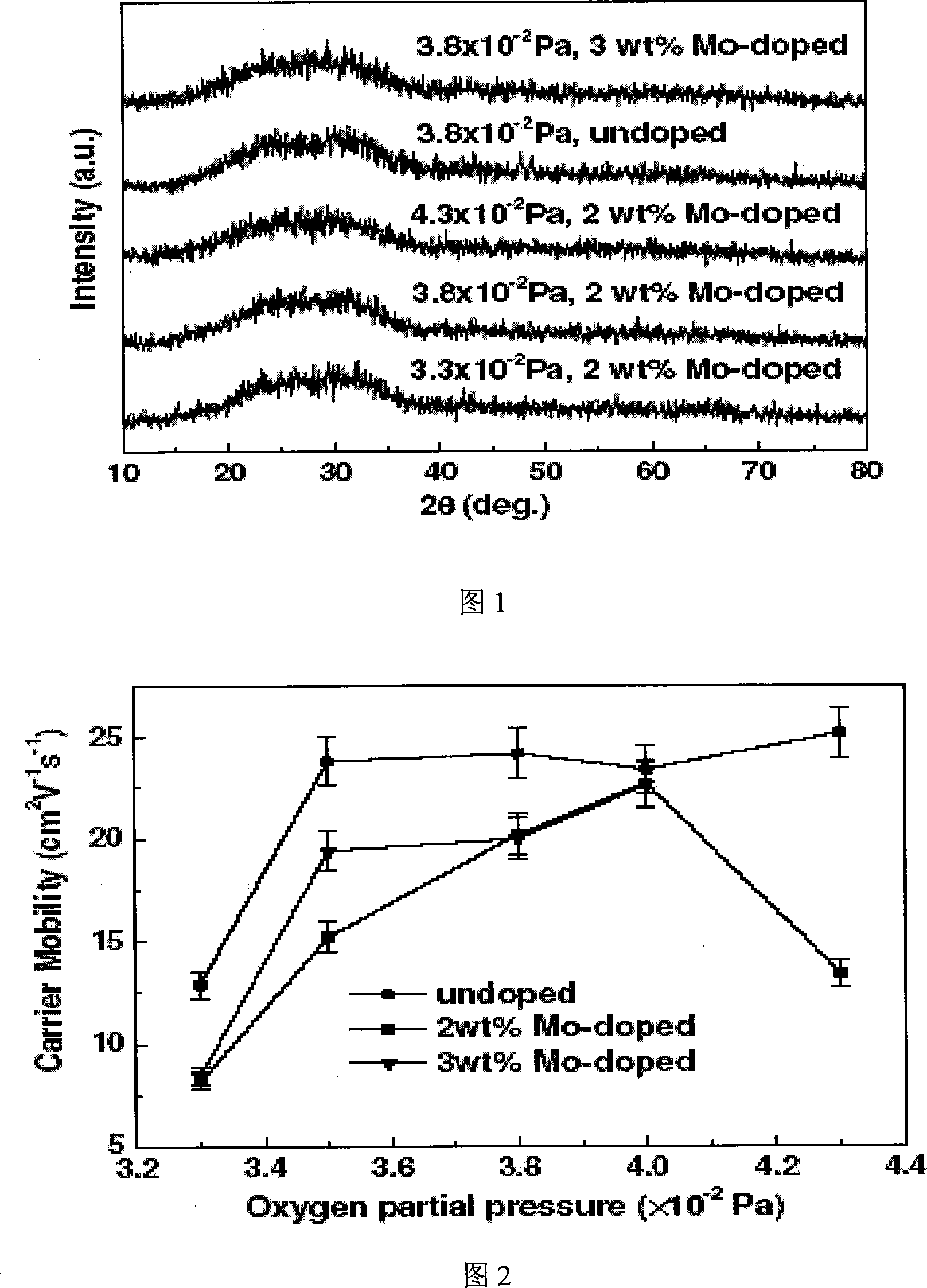
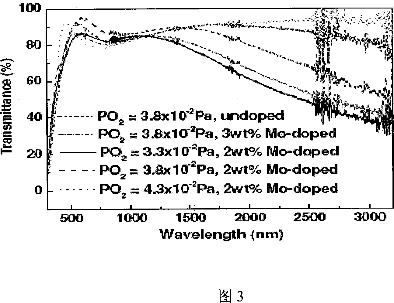
[0021] Example 1, preparation of molybdenum-doped indium oxide target: In metal with a purity of 99.99% is melted into a target, and 2 wt% of molybdenum wire with the same purity of 99.99% is uniformly and symmetrically embedded. The target diameter is 51mm and the thickness is 3.0mm . The substrate is a common glass slide, which has been washed by pure water, alcohol and acetone ultrasonic waves for 15 minutes each.
[0022] Substrate temperature: room temperature. The distance between the target and the substrate was fixed at 50mm. Before film deposition, the reaction chamber was evacuated to less than 2×10 -3 Pa, then the O through the variable air pilot valve 2 And Ar gas into the reaction chamber. The working pressure in the reaction chamber is 2.5×10 -1 Pa, sputtering current is 100mA, sputtering voltage is 350V, control O 2 The partial pressure of the reaction gas is 3.8×10 -2 Pa. Thin films were prepared on ordinary glass slides. The sputtering time is 10 minu...
Embodiment 2
[0023] Example 2, preparation of tungsten-doped indium oxide target: In metal with a purity of 99.99% is melted into a target, and 2 wt% of tungsten wire with the same purity of 99.99% is evenly and symmetrically embedded, and the target diameter is 51mm and the thickness is 3.0mm . The substrate is a common glass slide, which has been washed by pure water, alcohol and acetone ultrasonic waves for 15 minutes each.
[0024] Substrate temperature: room temperature. The distance between the target and the substrate was fixed at 50mm. Before film deposition, the reaction chamber was evacuated to less than 2×10 -3 Pa, then the O through the variable air pilot valve 2 And Ar gas into the reaction chamber. The working pressure in the reaction chamber is 3.0×10 -1 Pa, sputtering current is 150mA, sputtering voltage is 385V, control O 2 The partial pressure of the reaction gas is 3.5×10 -2 Pa. Thin films were prepared on ordinary glass slides. The sputtering time is 8 minutes,...
PUM
| Property | Measurement | Unit |
|---|---|---|
| Diameter | aaaaa | aaaaa |
| Thickness | aaaaa | aaaaa |
| Thickness | aaaaa | aaaaa |
Abstract
Description
Claims
Application Information
 - R&D Engineer
- R&D Manager
- IP Professional
- Industry Leading Data Capabilities
- Powerful AI technology
- Patent DNA Extraction
Browse by: Latest US Patents, China's latest patents, Technical Efficacy Thesaurus, Application Domain, Technology Topic, Popular Technical Reports.
© 2024 PatSnap. All rights reserved.Legal|Privacy policy|Modern Slavery Act Transparency Statement|Sitemap|About US| Contact US: help@patsnap.com