Inorganic EL display insulation media and its making method

A technology of insulating medium and manufacturing method, which is applied in the field of inorganic thin film electroluminescent display, and can solve the problems of reducing the interface polarization electric field, destroying the lower dielectric layer and light-emitting layer, and low brightness

Inactive Publication Date: 2008-02-13
INESA ELECTRON
View PDF0 Cites 8 Cited by
  • Summary
  • Abstract
  • Description
  • Claims
  • Application Information

AI Technical Summary

Problems solved by technology

The asymmetric structure is widely used in TDEL and is recognized as very successful. However, there are still many problems in the TFEL device with asymmetric insulating layer: 1) Asymmetric TFEL is a new device structure, the choice of upper and lower dielectric materials , thickness and deposition process need to do a lot of experimental work
3) Although it was reported 15 years ago that SrTiO sputtered by radio frequency magnetron 3 , BaTiO 3 As an insulating layer of TFEL, and optimized process parameters, but has not been applied in production so far
Therefore, it is necessary to try new deposition methods, such as the preparation of epitaxial single crystals, but the preparation of large-area thin films cannot be realized at present and the cost is unacceptable
4) The lower dielectric layer used to maintain polarization is made of high-resistance materials, such as Ta 2 o 5 , It has been confirmed that the device threshold voltage is high and the brightness is low
SrTiO 3 , BaTiO 3 , BST and other perovskite ferroelectric/dielectric films need high-temperature deposition or subsequent annealing to obtain good crystallinity, which will seriously damage the lower dielectric layer and light-emitting layer, and its breakdown mode is generally propagating , so, at least at present, it is difficult to obtain practical application
6) The medium used more frequently in previous work is Y 2 o 3 、Si 3 N 4

Method used


Image

  • Inorganic EL display insulation media and its making method
  • Inorganic EL display insulation media and its making method
  • Inorganic EL display insulation media and its making method

Examples


Embodiment 1

[0102] The structure of the device is ITO / BaTiO 3 (863nm)) / ZnS:Mn(300nm) / ATO(785nm) / Al. The substrate is NSG's STN-LCD glass or Corning's TFT-LCD glass. The lower electrode is an ITO electrode with a thickness of 150nm photolithography. The upper electrode is an electron-beam-evaporated aluminum electrode with a thickness of 150 nm. BaTiO 3 The deposition conditions: the background vacuum is 3.0×10 -3 Pa, the oxygen pressure is 3.0×10 -2 Pa, the rate is 2.5 Ȧ s -1 , the substrate temperature is 180°C. ATO deposition conditions: the background vacuum is 3.6×10 -3 Pa, O 2 Pressed to 3.2×10 -2 Pa, the substrate temperature is about 100°C, Al 2 o 3 The source evaporation rate is 3 Ȧ s -1 ,TiO 2 The source evaporation rate is 2.5 Å·s -1 , the substrate rotation rate is 1 rotation per 18 seconds. TiO 2 Cumulative thickness of 385nm, Al 2 o 3 The cumulative thickness was 400 nm. Deposition conditions of ZnS:Mn: the background vacuum is 3.9×10 -3 Pa, substrate temp...

Embodiment 2

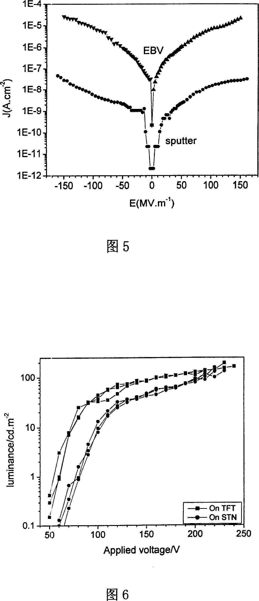
[0105] The structure of the device is STN glass / ITO / BaTiO 3 (300nm)) / ZnS:Mn(382nm) / ATO(730nm) / Al. Upper electrode Al, lower electrode ITO, BaTiO 3 , ZnS:Mn, the preparation conditions of ATO are the same as example 1. Fig. 7 shows the L-V relationship of one of the four pixels. L at 200Hz 50 209cd·m -2 , The optical threshold voltage is 110V.

Embodiment 3

[0107] Prepared a 2-inch 128×64ZnS:Mn matrix screen with a structure of STN glass / ITO / BaTiO 3 (860nm)) / ZnS:Mn(500nm) / ATO(730nm) / Al. The evaporation and annealing conditions of upper electrode Al, lower electrode ITO, ZnS:Mn, ATO are the same as Example 1. Evaporated BaTiO 3 The substrate temperature at the time was 112° C., and all the other conditions were the same as in Example 1. BaTiO 3 Before deposition, the substrate was coated with O 2 Plasma treatment was performed for 10 min to eliminate the photoresist that may remain on the surface of the substrate. L obtained at 200Hz 50 5cd·m -2 , The optical threshold voltage is 160V. Figure 8 shows the L-V curve.


PUM


Abstract

An inorganic electroluminescent display insulating medium and the manufacturing method comprise: a multi-layer composite thin film A1203/Ti02 and a AlxTiyOz thin film are manufactured as the medium layer on the ZnS:Mn ACTFEL device through electron beam evaporation method; Bati03 and SrTi03 thin films as the lower medium layer or the electric injection layer of ZnS:Mn ACTFEL device are manufactured and the follow-up annealing temperature of the BaTi03 thin film is reached through the electron evaporation method. The thin films are compared with the SrTi03 and Ba0.55Sr0.5Ti03 thin films manufactured through the traditional sputtering method. The invention optimizes the technique environment of pulse reactive sputtering A1203 thin film, comprising the power, pressure and oxygen content, and is appied to the ZnS:Mn four-pixel devices and the two-inch 128*64 matrix, obtaining better brightness effect. Mediums used in manufacturing the devices comprise Ba0.5Sr0.5TiO3 question mark SrTiO3 question mark BaTiO3 question mark HfO2 question mark Al2O3 question mark Ta2O5 question mark ZrO2 thin films by electron beam evaporation, radio frequency magnetron sputtering or impulse reactive sputtering.

Description

technical field [0001] The invention belongs to the technical field of AC-driven inorganic thin-film electroluminescent display, in particular to a deposition method and an improved process for a medium used in an inorganic thin-film electroluminescent display. Background technique [0002] Electroluminescence refers to the phenomenon that a solid material emits light under the action of a DC or AC electric field, relying on the excitation of current and electric field. Inorganic thin film electroluminescent display (TFEL) has full curing, active luminescence, wide viewing angle (>160°), fast response speed (μs order), large contrast ratio (100:1), high resolution (1000lpi), wide operating temperature (-25-65°C), strong shock resistance, long life (>10 5 h) and other advantages, it is one of the next-generation flat panel display technologies with superior comprehensive performance and wide application prospects. The structure of the TFEL display is usually a MISIM (...

Claims


Application Information

Patent Timeline
IPC IPC(8): H01L33/00H01L27/15H01L21/31H01L21/316C23C14/00C23C14/30C23C14/34
Inventor 黄浩肖田林明通徐毅
Owner INESA ELECTRON
Why Eureka
Try Eureka