Non mask preparation method based on thin film multiple layer film nano magnetic electron device
A technology for electronic devices and multilayer films, which is applied in the manufacture/assembly of piezoelectric/electrostrictive devices, the manufacture/assembly of magnetostrictive devices, and the manufacture/processing of electromagnetic devices, etc. Complex, unsuitable for single-piece, small batch production and other problems, to achieve the effect of simple method and high efficiency
- Summary
- Abstract
- Description
- Claims
- Application Information
AI Technical Summary
Problems solved by technology
Method used
Image

Examples
Embodiment 1
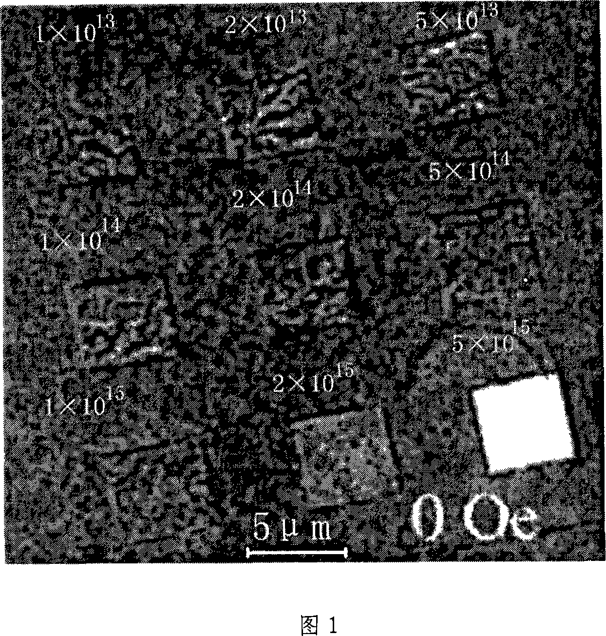
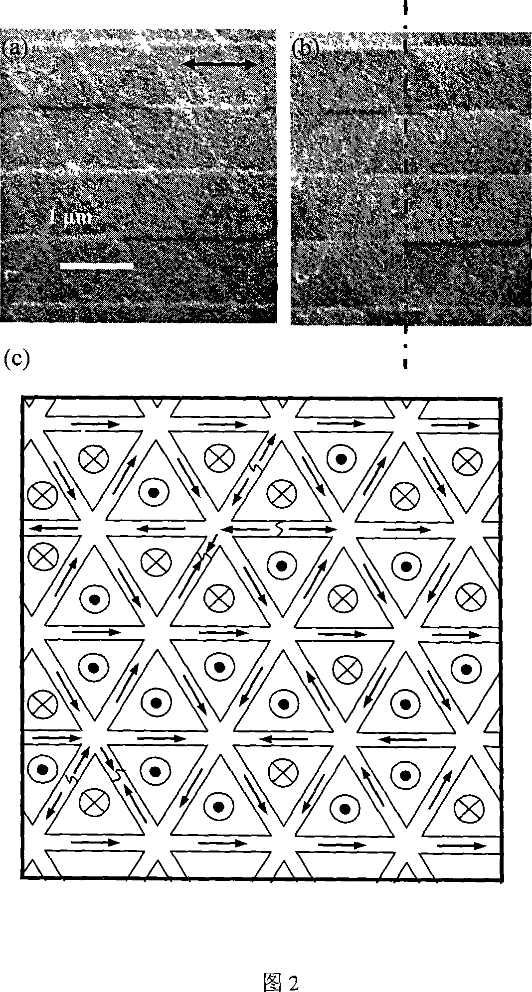
[0021] Embodiment 1, preparation of magnetoelectronic devices based on Pt / Co magnetic recording multilayer film by maskless method
[0022] Pt(2.8nm) / [Pt(0.6nm) / Co(0.3nm)] was sequentially deposited on a 1mm thick single crystal silicon substrate cleaned by conventional methods using high-vacuum magnetron sputtering equipment 6 / Pt (6.5nm). The growth conditions of the above-mentioned magnetic multilayer film: prepared vacuum: 5×10 -7 Pa; high-purity argon gas pressure for sputtering: 7×10 -2 Pa; sputtering power: 120W; sample holder rotation rate: 20rpm; growth temperature: room temperature; growth rate: 0.03-0.12nm / s. The deposited magnetic multilayer film is micro-nano-processed using a focused ion beam workstation, and the dose of gallium ion irradiation is 1×10 13 ~5×10 14 ions / cm 2 , Gallium ions are vertically incident on the surface of the magnetic film, the ion beam energy is 30keV, and the ion beam current is 1nA. First, the control program of the ion beam and ...
Embodiment 2
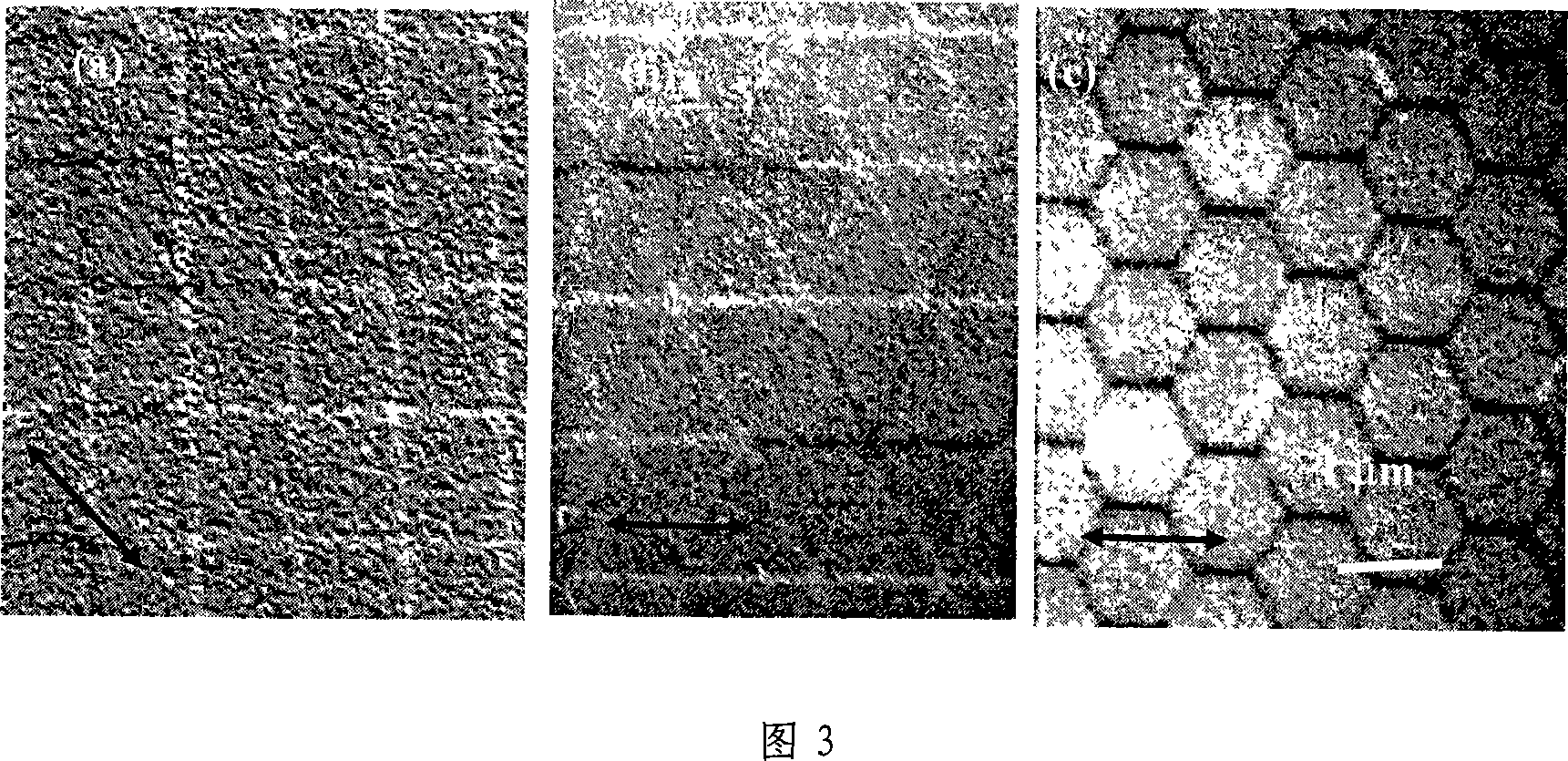
[0023] Embodiment 2, preparation of magnetic electronic devices based on CoFe ferromagnetic thin film by maskless method
[0024] A lower buffer layer Ta with a thickness of 5 nm, a CoFe ferromagnetic layer with a thickness of 10 nm and a protective layer Ta with a thickness of 10 nm were deposited on a 1 mm thick single crystal silicon substrate cleaned by a conventional method using a high vacuum magnetron sputtering device. The growth conditions of the above-mentioned magnetic film: prepared vacuum: 5×10 -7 Pa; high-purity argon gas pressure for sputtering: 7×10 -2 Pa; sputtering power: 120W; sample holder rotation rate: 20rpm; growth temperature: room temperature; The deposited magnetic thin film is micro-nano-fabricated using a focused ion beam workstation, and the dose of gallium ion irradiation is 1×10 14 ~1×10 15 ions / cm 2, Gallium ions are vertically incident on the surface of the magnetic film, the ion beam energy is 30keV, and the ion beam current is 1nA. First...
Embodiment 3
[0025] Embodiment 3, the magnetic electronic device based on FeNi ferromagnetic thin film is prepared by maskless method
[0026] A lower buffer layer Ta with a thickness of 5nm, a FeNi ferromagnetic layer with a thickness of 10nm and a protective layer Ta with a thickness of 10nm were deposited on a 1mm thick single crystal silicon substrate cleaned by a conventional method using high vacuum magnetron sputtering equipment. The growth conditions of the above-mentioned magnetic film: prepared vacuum: 5×10 -7 Pa; high-purity argon gas pressure for sputtering: 7×10 -2 Pa; sputtering power: 120W; sample holder rotation rate: 20rpm; growth temperature: room temperature; The deposited magnetic thin film is micro-nano-processed using a focused ion beam workstation, and the dose of ion irradiation is 1×10 14 ~1×10 15 ions / cm 2 , the ion beam energy is 30keV, and the ion beam current is 1nA. First, upload the control program of the ion beam and the sample stage on the focused ion ...
PUM
| Property | Measurement | Unit |
|---|---|---|
| Thickness | aaaaa | aaaaa |
| Thickness | aaaaa | aaaaa |
| Thickness | aaaaa | aaaaa |
Abstract
Description
Claims
Application Information
 - R&D
- Intellectual Property
- Life Sciences
- Materials
- Tech Scout
- Unparalleled Data Quality
- Higher Quality Content
- 60% Fewer Hallucinations
Browse by: Latest US Patents, China's latest patents, Technical Efficacy Thesaurus, Application Domain, Technology Topic, Popular Technical Reports.
© 2025 PatSnap. All rights reserved.Legal|Privacy policy|Modern Slavery Act Transparency Statement|Sitemap|About US| Contact US: help@patsnap.com