Check patentability & draft patents in minutes with Patsnap Eureka AI!

Interferometer and method of use thereof

An interferometer and micro-moving platform technology, applied in the field of interferometers, can solve the problems of large volume adjustment of interferometers, complicated manufacturing and installation, and difficulty in wave aberration detection, and achieve convenient movement, reduce volume, increase reliability and The effect of stability

Active Publication Date: 2008-05-21
SHANGHAI MICRO ELECTRONICS EQUIP (GRP) CO LTD
View PDF0 Cites 13 Cited by
  • Summary
  • Abstract
  • Description
  • Claims
  • Application Information

AI Technical Summary

Problems solved by technology

However, the main disadvantages of this online detection objective lens method are: 1: The laser light source uses two sets of beam expander and attenuation systems, resulting in a large number of optical components, complex structure, and complicated manufacturing and assembly; 2: Converging lens groups and spherical reflections are required In this way, more measurement errors are introduced. Although this measurement error can realize self-calibration, if there are too many errors, there will be large errors in the calibration itself; 3: The system introduces a special alignment system , although it can achieve fast measurement, it requires more optical components and another imaging system, which increases the complexity of the system; 4: The objective lens test often needs to check the optical characteristics of different points on the entire object surface, due to the The volume is large and it is inconvenient to move, and the interferometer itself is also large and inconvenient to adjust, which makes it difficult to detect the wave aberration of different object image points of the objective lens

Method used


Image

  • Interferometer and method of use thereof
  • Interferometer and method of use thereof
  • Interferometer and method of use thereof

Examples


Embodiment Construction

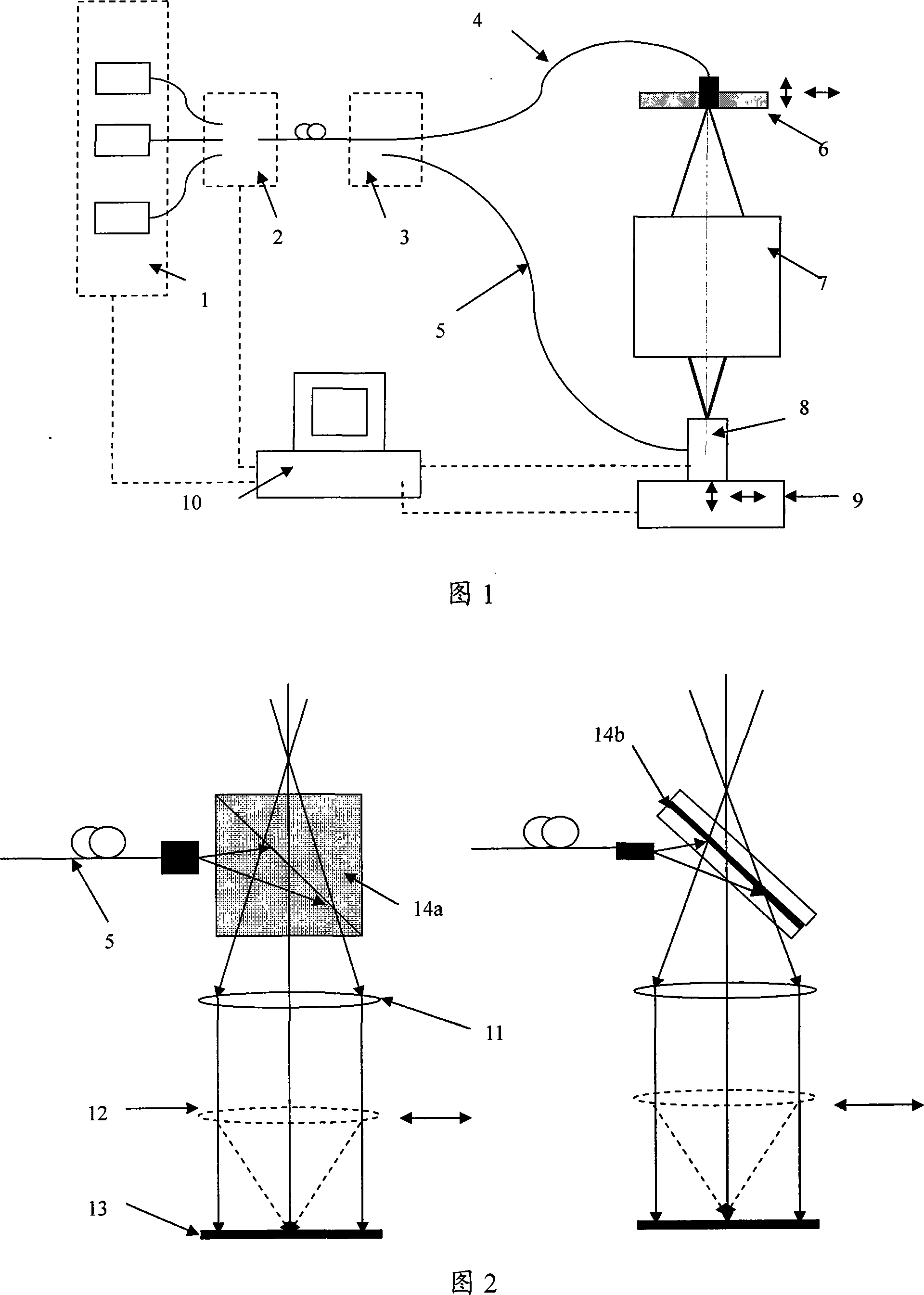
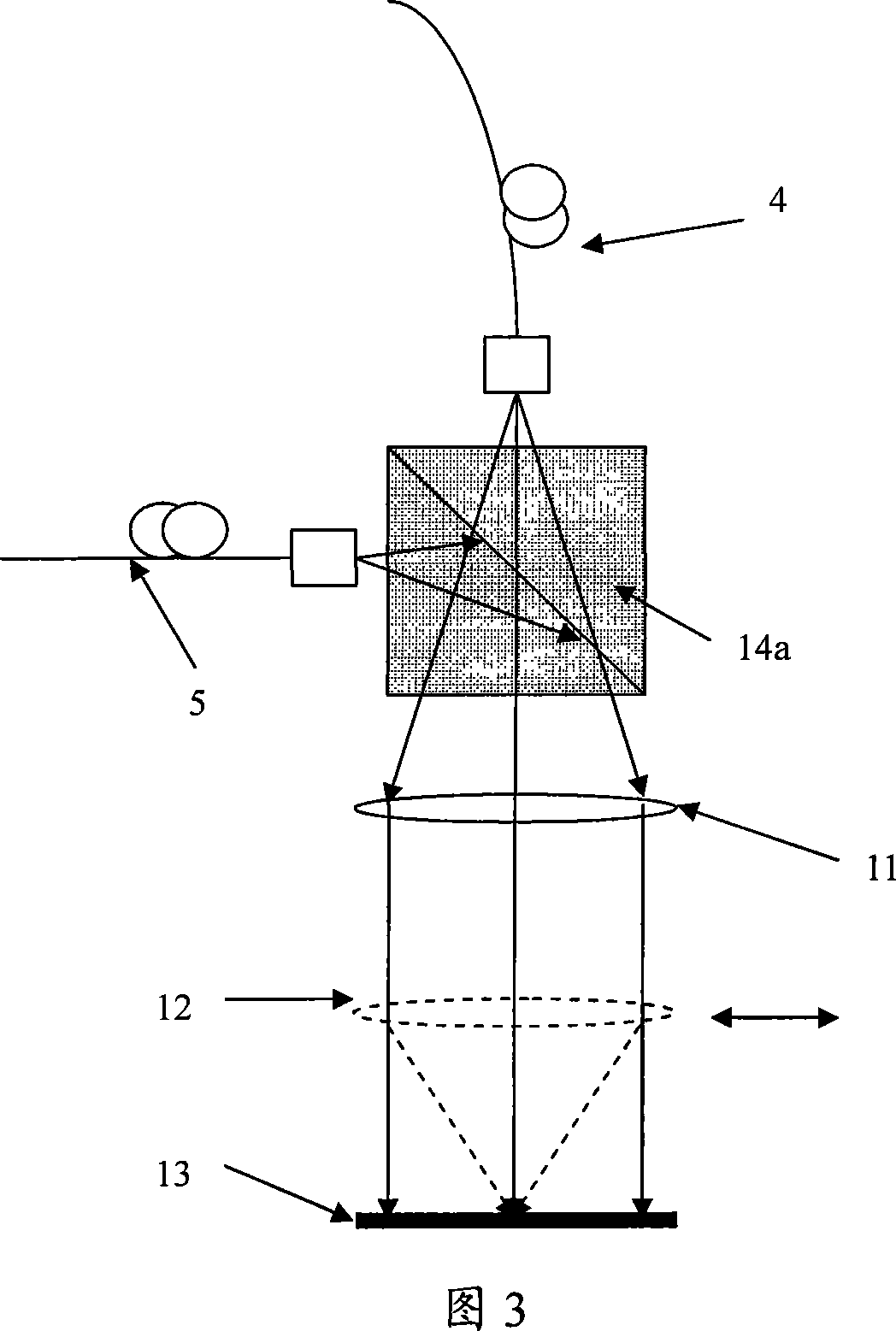
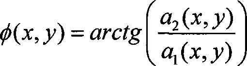
[0032] The interferometer of the present invention uses an optical fiber as a transmission optical path to generate a standard wavefront, and adopts a common path interference system to realize the aberration detection of the projection objective lens of the encapsulated lithography machine. The specific device is as follows:

[0033] First, please refer to Figure 1. Figure 1 is a schematic diagram of the structure of the interferometer of the present invention. The laser light source module 1 contains three semiconductor lasers with wavelengths of 375nm, 405nm and 436nm. These three wavelengths basically cover the working bandwidth of the objective lens under test. Each semiconductor laser is coupled to a single-mode fiber for output. In order to obtain a standard diffracted wavefront, the single-mode fiber chooses a smaller core size; the optical switch 2 is connected to the laser light source module 1 through a single-mode fiber; After switch 2 is splitter module 3, splitter mo...


PUM


Abstract

The invention discloses an interferometer for detecting a projection lens of a post-encapsulated lithography machine and a use method thereof. The interferometer of the invention comprises a laser light source module which produces the light source, a single mode fiber which connects the laser light source module with an optical switch, a light splitting module which is connected with the optical switch through the single mode fiber, an optical imaging system receiving the light source, an image sensor and a main control computer which is connected with each component of the interferometer. When in use of the interferometer, the measured objective lens is arranged between the light splitting module and the optical imaging system receiving the light source; the key point of the invention is as follows that an optical fiber position adjustment module is arranged between the light splitting module and the measured objective lens and an interference module is arranged behind the measured objective lens, moreover, the interferometer is arranged on a micro-motion bench of the lithography machine. The interferometer of the invention can accurately measure the wave-front error of the projection lens of the post-encapsulated lithography machine and reduce the size of the optical detecting component; moreover, the invention has simple manufacture, high detection precision and easy operation.

Description

Technical field [0001] The invention relates to an interferometer, in particular to an interferometer used for detecting the wave aberration of a projection objective lens of a rear-packing lithography machine. Background technique [0002] In recent years, in the field of semiconductor lithography, projection lithography technology has continued to advance, and lines have advanced in a finer direction. Post-exposure packaging lithography machines have been widely used due to their high yield and no damage to the mask. The post-exposure packaging lithography machine usually has a magnification of 1x and a numerical aperture below 0.4. The wavelength usually selects the ghi three-line or single-line wavelength working mode. The quality of the lithography objective is a key factor affecting the overall performance of the post-package lithography machine. Projection objectives can be designed to achieve high quality, but the optical quality of the objective lens will be affected in ...

Claims


Application Information

Patent Timeline
Patent Type & Authority Applications(China)
IPC IPC(8): G01M11/02G01J9/02
Inventor 刘国淦
Owner SHANGHAI MICRO ELECTRONICS EQUIP (GRP) CO LTD
Features
  • R&D
  • Intellectual Property
  • Life Sciences
  • Materials
  • Tech Scout
  • Unparalleled Data Quality
  • Higher Quality Content
  • 60% Fewer Hallucinations
Learn More