Integrated opto-electronic device for generating high-frequency microwave by light heterodyne method

An optoelectronic device and high-frequency microwave technology, applied in the field of microwave photonics, can solve the problems of short transmission distance, high absorption loss and high cost, and achieve the effect of monolithic integration

Inactive Publication Date: 2008-07-16
TSINGHUA UNIV
View PDF0 Cites 18 Cited by
  • Summary
  • Abstract
  • Description
  • Claims
  • Application Information

AI Technical Summary

Problems solved by technology

[0006] 2. Short transmission distance: the 60 GHz band is in the strong absorption area of ​​oxygen, and its absorption loss is as high as 16dB / km
As we all know, the systems built by discrete devices are often large and complex, with poor stability and relatively high cost.

Method used


Image

  • Integrated opto-electronic device for generating high-frequency microwave by light heterodyne method
  • Integrated opto-electronic device for generating high-frequency microwave by light heterodyne method

Examples


Embodiment 1

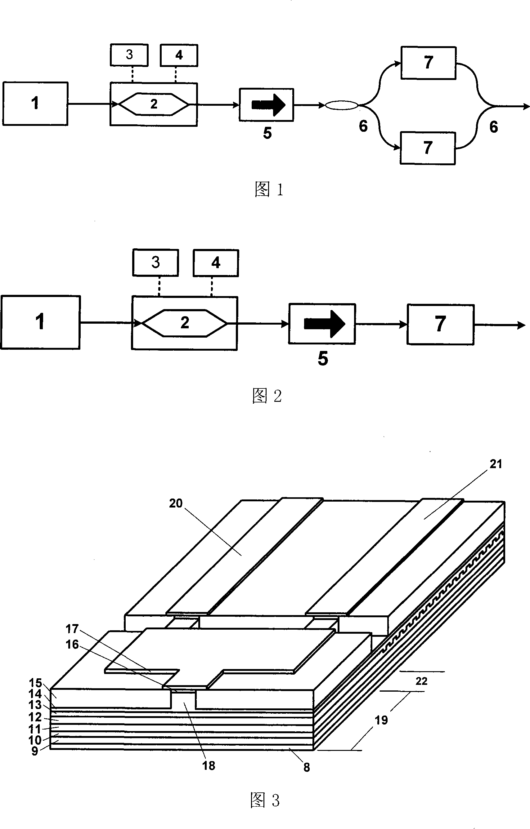
[0044] Embodiment 1 An InGaAsP / InP-based single-ended MMI coupled photo-generated microwave integrated device with an operating wavelength within the 1550nm band (the structure shown in FIG. 3 ).

[0045] The epitaxial materials for the devices are described below. First, an epitaxial, n-type InP buffer layer (thickness 200nm, doping concentration about 1×10 18 cm -2 ), 100nm thick undoped lattice-matched InGaAsP waveguide layer (photoluminescence wavelength 1.2μm), strained InGaAsP multiple quantum wells (photoluminescence wavelength 1.52μm, 7 quantum wells: well width 8nm, 0.5% compressive strain, barrier width 10nm , Lattice matching material, photofluorescence wavelength 1.2μm), 70nm thick InGaAsP grating material layer. Next, the grating structure is fabricated by holographic interference exposure, and the grating in the MMI region is removed by photolithography and wet etching. Then secondary epitaxial 100nm thick p-type lattice matching InGaAsP waveguide layer (light...

Embodiment 2

[0048] Embodiment 2 An InGaAsP / InP-based double-terminal MMI coupled photo-generated microwave integrated device with an operating wavelength within the 1550nm band (the structure shown in FIG. 4 ).

[0049] The epitaxial materials for the devices are described below. First, an epitaxial, n-type InP buffer layer (thickness 200nm, doping concentration about 1×10 18 cm -2 ), 100nm thick undoped lattice-matched InGaAsP waveguide layer (photoluminescence wavelength 1.2μm), strained InGaAsP multiple quantum wells (photoluminescence wavelength 1.52μm, 7 quantum wells: well width 8nm, 0.5% compressive strain, barrier width 10nm , Lattice matching material, photofluorescence wavelength 1.2μm), 70nm thick InGaAsP grating material layer. Next, the grating structure is fabricated by holographic interference exposure, and the grating in the MMI region is removed by photolithography and wet etching. Then secondary epitaxial 100nm thick p-type lattice matching InGaAsP waveguide layer (li...

Embodiment 3

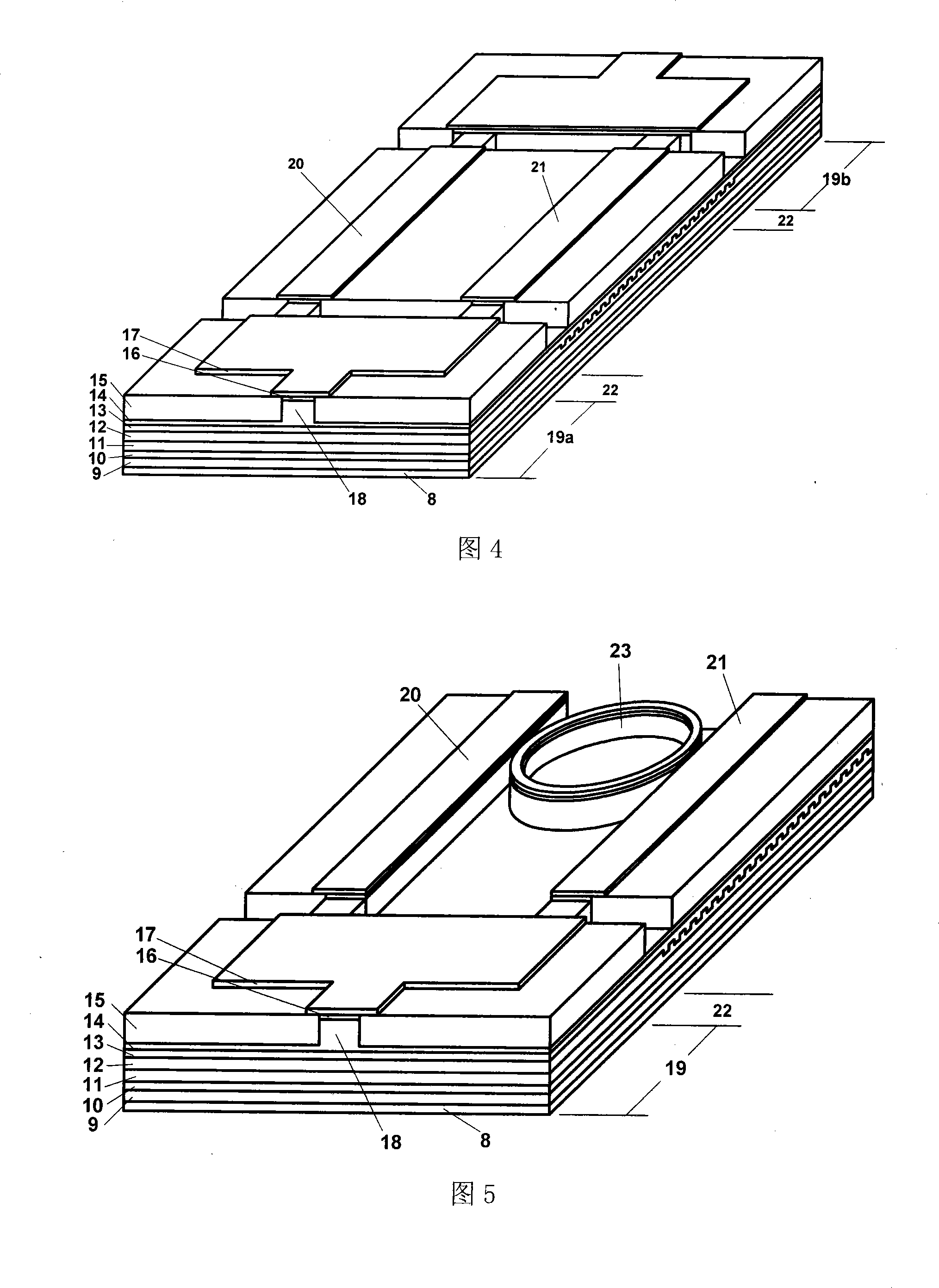
[0052] Embodiment 3 An InGaAsP / InP-based microring-coupled photo-generated microwave integrated device with an operating wavelength in the 1550nm band (the structure shown in FIG. 5 ).

[0053] The epitaxial materials for the devices are described below. First, an epitaxial, n-type InP buffer layer (thickness 200nm, doping concentration about 1×10 18 cm -2 ), 100nm thick undoped lattice-matched InGaAsP waveguide layer (photoluminescence wavelength 1.2μm), strained InGaAsP multiple quantum wells (photoluminescence wavelength 1.52μm, 7 quantum wells: well width 8nm, 0.5% compressive strain, barrier width 10nm , Lattice matching material, photofluorescence wavelength 1.2μm), 70nm thick InGaAsP grating material layer. Next, the grating structure is produced by holographic interference exposure, and the grating in the microring and MMI area is removed by photolithography and wet etching. Then secondary epitaxial 100nm thick p-type lattice matching InGaAsP waveguide layer (light ...


PUM

PropertyMeasurementUnit
Lengthaaaaaaaaaa

Abstract

The invention belongs to the photoelectronic device preparation technical range in the microwave photonics field, in particular relates to an integrated photoelectronic device which utilizes an optical heterodyne method to generate high-frequency microwaves. A main laser and a slave laser of the integrated photoelectronic device are parallelly arranged on a substrate on which a lower optical guiding layer, an MQW active layer, a grating layer, an upper optical guiding layer, an upper cladding and an ohmic contact layer are orderly extended outwards and integrated together; one end of the main laser and one end of the slave laser realize coupling of modulation sidebands through a multimode interferometer or an annulet structure, and injection locking is performed; then coupling out is performed by the multimode interferometer, heterodyne is performed, the high-frequency microwaves can be obtained. Therefore, differences of laser radiated wavelengths are realized by means of controlling working temperature and injection current of a DFB laser, thereby achieving the effect of injection locking of sidebands. The invention has a novel structure and simple production process, and has broad application prospect in the future high-speed communication field.

Description

technical field [0001] The invention belongs to the technical scope of preparation of optoelectronic devices in the field of microwave photonics, and in particular relates to an integrated optoelectronic device for generating high-frequency microwaves by using an optical heterodyne method. technical background [0002] Integrated optoelectronic devices that use optical heterodyne to generate high-frequency microwaves have a wide range of applications, including wireless local area networks, antenna remote control, etc. The following first briefly introduces the importance of high-frequency microwave or millimeter wave in wireless communication, and then introduces the application of optoelectronic technology in millimeter wave wireless communication. [0003] In recent years, with the continuous development of optical fiber networks and the Internet (Internet), voice, image, data, video, and multimedia services based on the Internet have greatly stimulated people's demand fo...

Claims


Application Information

Patent Timeline
IPC IPC(8): H01S5/026H01S5/40H01S5/06H01S5/125H01S5/065H01S5/00H01S1/00
Inventor 孙长征黄缙熊兵罗毅
Owner TSINGHUA UNIV
Why Eureka
Try Eureka