

Method for forming grounding via hole between gallium nitride device and circuit
A gallium nitride device, gallium nitride technology, applied in circuits, electrical solid state devices, semiconductor devices, etc., can solve problems such as inability to etch, achieve the effects of eliminating parasitic inductance, simple operation, and easy implementation
- Summary
- Abstract
- Description
- Claims
- Application Information
AI Technical Summary
Problems solved by technology
Method used
Image

Examples
Embodiment 1
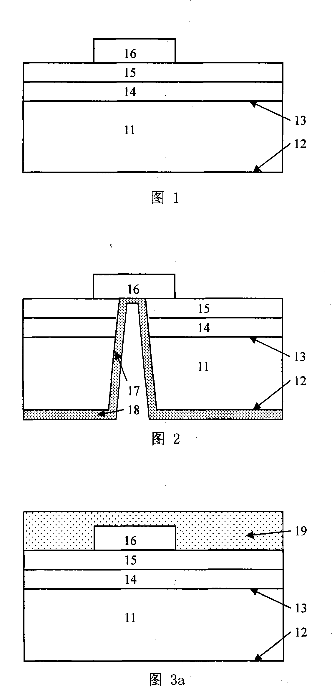
[0049] figure 1 Shown in the present invention is the aluminum gallium nitride / gallium nitride heterojunction material on the SiC substrate used to etch through holes and the devices or circuits on it (for simplicity, only one electrode is drawn) A cross-sectional view, which includes a SiC substrate 11 having a surface 12 and a surface 13, a gallium nitride buffer layer 14 on the surface 13 of the SiC substrate, and an aluminum gallium nitride barrier layer 15 and a barrier layer 15 formed thereon 上Formed electrode 16. The substrate 11 is generally 300-500 μm, the thickness of the gallium nitride buffer layer 14 is generally 1 to 3 μm, and the thickness of the aluminum gallium nitride barrier layer 15 is 15-30 nm.
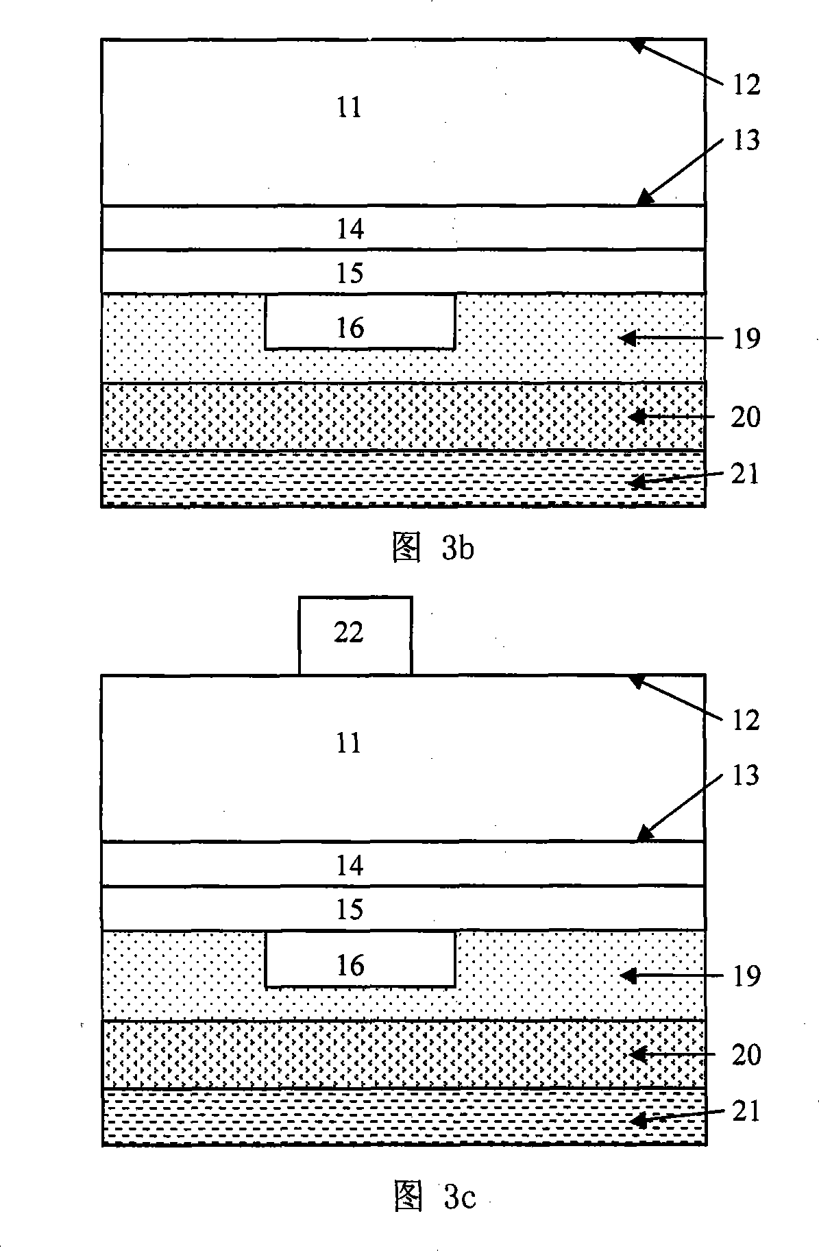
[0050] figure 1 The surface of the epitaxial layer and the electrode 16 are coated with polymer 19, such as Figure 3a As shown in the figure, the role of polymer 19 is on the one hand to protect the devices or circuits below it from being damaged in the subsequent pr...
Embodiment 2
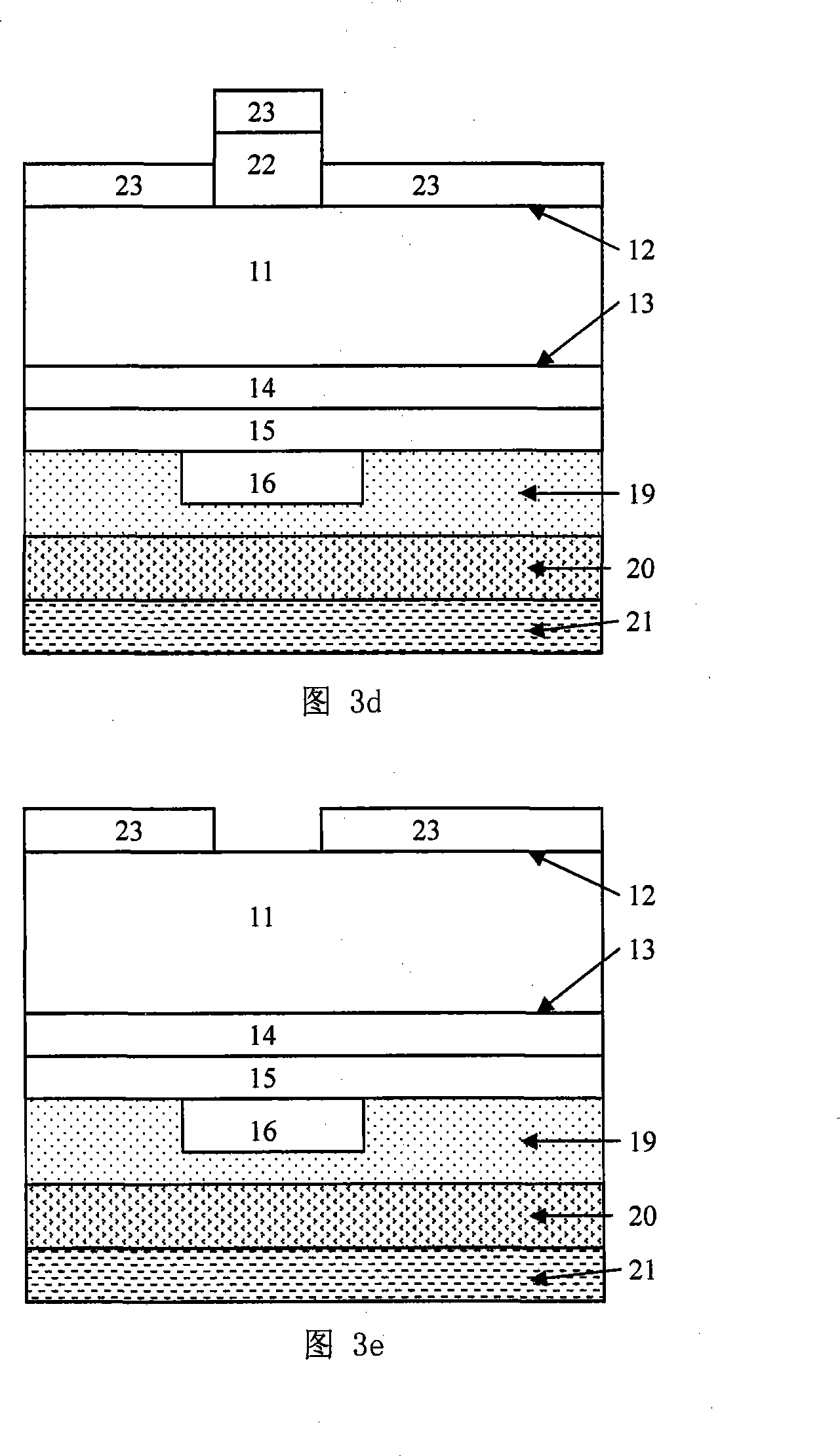
[0063] reference Figure 3a-3b First, the surface of the substrate 11 is coated with a polymer 19 to protect the devices or circuits on it, and then it is mounted upside down on the platen 21 and filled with an adhesive 20, and then the substrate 11 is thinned to Between 50 and 100 μm, the specific implementation of this process is the same as in Example 1, and will not be detailed here.
[0064] After the substrate 11 is thinned, a metal photoetching mark is made thereon, and the role of the photoetching mark is to facilitate photolithography alignment in subsequent processes. The preferred photolithography mark formation process in this embodiment includes coating photoresist on the surface 12 of the substrate 11, exposing and developing the photoresist on the mask with ultraviolet light. The marking pattern is transferred to the photoresist, and then the Ti / Au is evaporated by electron beam and peeled off to form a photolithography mark on the surface 12 of the substrate 11.
...
PUM
| Property | Measurement | Unit |
|---|---|---|
| thickness | aaaaa | aaaaa |
| thickness | aaaaa | aaaaa |
| thickness | aaaaa | aaaaa |
Abstract
Description
Claims
Application Information