Schottky indoor temperature nucleus radiation detector and its making method

A nuclear radiation detector, Schottky-type technology, applied in semiconductor devices, electrical components, circuits, etc., can solve the problems of low thermal conductivity of CZT crystal materials, complex preparation process, increase detector manufacturing cost, etc., to achieve good mechanical Effects of performance and chemical stability, mature material growth process, and good room temperature sensitivity

Inactive Publication Date: 2008-08-13
SUZHOU INST OF NANO TECH & NANO BIONICS CHINESE ACEDEMY OF SCI
View PDF0 Cites 5 Cited by
  • Summary
  • Abstract
  • Description
  • Claims
  • Application Information

AI Technical Summary

Problems solved by technology

[0004] At present, the CdZnTe (CZT) room temperature nuclear radiation detector is the most researched. The United States, Russia and other countries have commercialized the CZT crystal material and its detector. However, the crystal material has the following problems: ① Due to the thermal conductivity of the CZT crystal material It is extremely low, and its stacking defect formation energy is small, so that during the crystal growth process, factors such as temperature fluctuations can easily cause the appearance of twins; ②Due to its low critical shear stress, it is easy to generate dislocations; ③Its constituent elements Among them, the vapor partial pressure of Cd is much higher than that of the other two components, and it is easy to cause the melt to be rich in Te; ④ During the cooling proces

Method used


Image

  • Schottky indoor temperature nucleus radiation detector and its making method

Examples


Embodiment 1

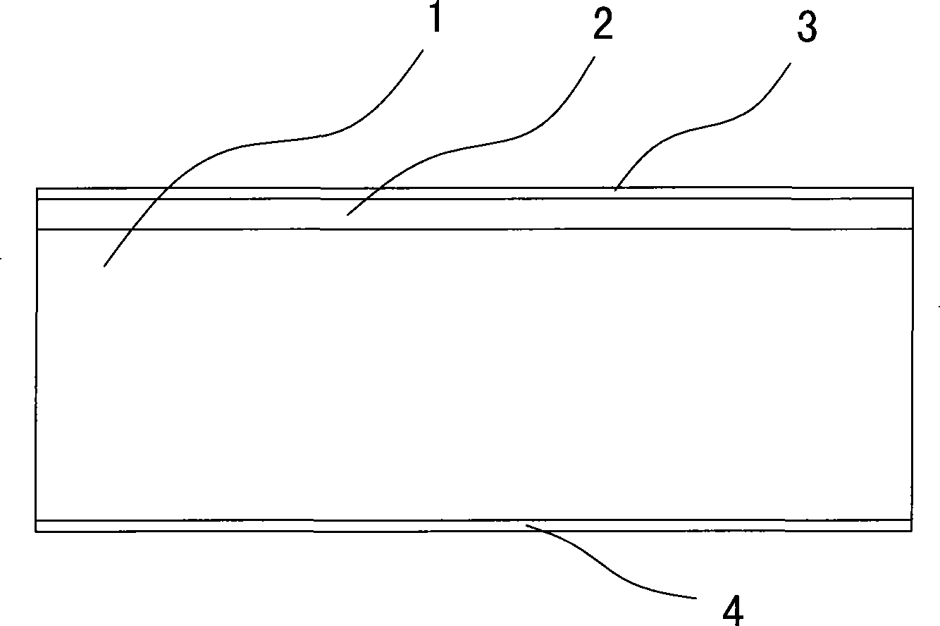
[0027] Embodiment one: see attached figure 1 As shown, a Schottky-type room temperature nuclear radiation detector includes a Schottky structure, a Schottky electrode and an ohmic electrode formed by a GaN substrate, and the GaN substrate is composed of a GaN single crystal thick film substrate 1 and an n-type The doped layer 2 is composed of a thickness of 100um-200um and 2um respectively, the ohmic contact electrode 3 is arranged on the surface of the n-type doped layer 2, and the Schottky junction electrode 4 is arranged on the surface of the other side of the substrate.

[0028] Wherein, the resistivity of the GaN substrate is 10 6 ~10 9 Ω cm, dislocation density less than 10 6 cm -2 .

[0029] The electrodes are contact electrodes made by depositing 10nm / 30nm Ti / Au and 20nm Pd or Au respectively on the two surfaces of the GaN substrate.

[0030] The preparation method of the above-mentioned Schottky type room temperature nuclear radiation detector comprises the follo...


PUM

PropertyMeasurementUnit
Thicknessaaaaaaaaaa
Resistivityaaaaaaaaaa
Dislocation densityaaaaaaaaaa

Abstract

The present invention discloses a schottky type room temperature nuclear radiation detector which comprises a schottky structure formed by the GaN substrate, a schottky electrode and an ohmic electrode, and the invention that the following characters: the GaN substrate is a thick film structure with thickness 100um to 200um, the schottky electrode and ohmic electrode are respectively arranged at surface at two sides of the GaN substrate. As the GaN material used in the invention has the following excellent capabilities of broad forbidden band width, high resistivity, large atomic number, better covalent bond combination, high melting point, high breakdown electric field, anti-corrosion and radiation resistance, the prepared room temperature nuclear radiation detector has excellent room temperature sensitiveness, detection efficiency and stability, and is more suitable for the detecting field of the high-radiation field. At the same time the manufacturing technique is simple and cost is low, and the invention is suitable to be industrially generalized.

Description

technical field [0001] The invention relates to a nuclear radiation detector and a preparation method thereof, in particular to a Schottky-type GaN room temperature nuclear radiation detector and a preparation method thereof. Background technique [0002] Room temperature nuclear radiation detectors are a new type of detectors developed after gas detectors and scintillator detectors. They have high room temperature sensitivity, low noise, wide response spectrum, short pulse time, high detection efficiency, and radiation damage resistance. Strong, high stability and other advantages, it has a wide range of applications in the fields of environmental monitoring, nuclear medicine, industrial non-destructive testing, safety inspection, nuclear weapon penetration, aerospace, astrophysics and high-energy physics, and has become a frontier research hotspot in the modern high-tech field one. [0003] Since room temperature nuclear radiation detectors are required to work at room te...

Claims


Application Information

Patent Timeline
IPC IPC(8): H01L31/118H01L31/18
Inventor 陆敏
Owner SUZHOU INST OF NANO TECH & NANO BIONICS CHINESE ACEDEMY OF SCI
Why Eureka
Try Eureka