Preparation of strained germanium thin film

A technology of straining germanium and thin films, which is applied in semiconductor/solid-state device manufacturing, electrical components, circuits, etc., can solve the problems of not being able to use large-scale production, increase costs, consume materials, etc., and achieve the effect of improving performance

Inactive Publication Date: 2008-08-20
TSINGHUA UNIV
View PDF1 Cites 18 Cited by
  • Summary
  • Abstract
  • Description
  • Claims
  • Application Information

AI Technical Summary

Problems solved by technology

Thick SiGe buffer layers have several notable drawbacks associated with them: First, thick SiGe buffer layers are generally not easily integrated with existing Si-based CMOS processes
Second, it consumes a lot of materials, which greatly increases the cost
Cannot be used in mass production

Method used


Image

  • Preparation of strained germanium thin film
  • Preparation of strained germanium thin film
  • Preparation of strained germanium thin film

Examples


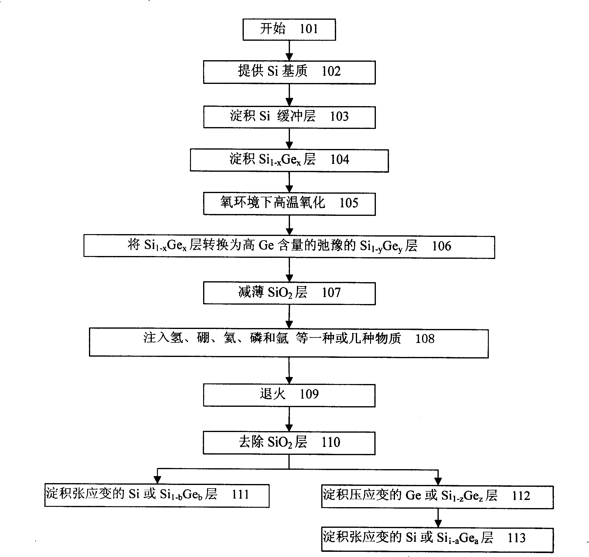
Embodiment example 1

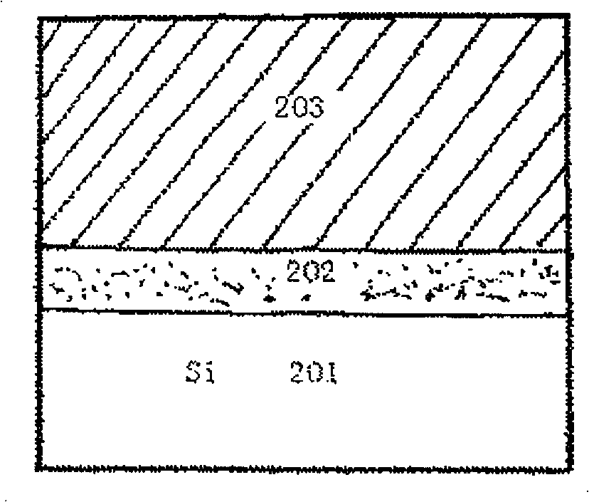
[0054] figure 2 Shown is strained single crystal silicon germanium (Si 1-x Ge x ) Schematic diagram of the cross-section of the substrate. Provided is a strained single crystal silicon germanium (Si 1-x Ge x ) process diagram of the production method of the layer substrate, covering a thickness of 200A on the Si substrate 201 0 The Si buffer layer 202, on the Si buffer layer 202 covers a layer of strained single crystal germanium silicon (Si 1-x Ge x ) layer 203, wherein, Si 1-x Ge x The thickness of the layer is 500A 0 , x=0.3.

Embodiment example 2

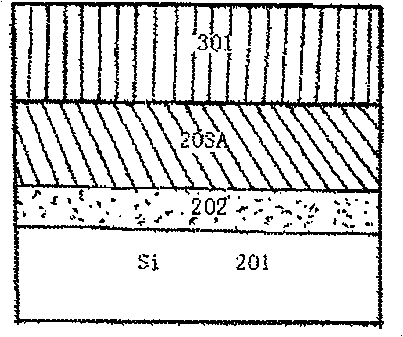
[0056] image 3 Shown is single crystal Si strained by high temperature oxidation 1-x Ge x layer 203, forming a relaxed single crystal Si 1-y Ge y The cross-sectional view of layer 203A and a layer of silicon dioxide film 301, using the method of high temperature oxidation, the strained single crystal germanium silicon (Si 1-x Ge x ) layer substrate 203 is transformed into relaxed Si with high Ge content 1-y Ge y layer 203A and a layer of silicon dioxide film 301, where y=0.6.

[0057] The oxidation environment is dry oxygen, and the oxidation temperature is between germanium silicon (Si 1-x Ge x ) The oxidation rate of the layer 203 is higher than the diffusion rate of Ge atoms in the range. Generally, the higher the temperature, the shorter the oxidation time required, and at the same time, the formed Si with high Ge content 1-y Ge y The Ge concentration in layer 203A is lower. Generally, the oxidation temperature is 900°C, and the oxidation time is 180 minutes. ...

Embodiment example 3

[0059] Such as Figure 4 As shown, for SiGeSi that is not fully relaxed 1-y Ge y Layer 203A is ion-implanted and annealed to form a fully relaxed silicon germanium Si 1-y Ge y Layer 203B. The SiO2 layer 301 is appropriately thinned to form 301A, so as to reduce the implantation energy.

[0060] Si implanted with argon ions 1-y Ge y Layer 203A consists of: 1 x 10 12 / cm 2 The dose is implanted in the energy range of 100keV.

[0061] Annealing includes annealing at a temperature of 800° C. for 60 minutes. Typically, annealing is performed in an atmosphere such as vacuum, nitrogen, argon, or other inert gas.


PUM


Abstract

The invention discloses a preparing method for strained germanium, belonging to the field of semiconductor substrate preparation. Single crystal silicon buffer layer is deposited on a silicon substrate; the single crystal silicon buffer layer is covered with a strained single crystal silicon germanium Si1-Gex layer having a thickness less than the critical thickness, then oxidized, and converted into a relax high-germanium component Si1-yGey layer; the high-germanium component Si1-yGey layer is completely relaxed by ion injection and annealing, and covered with compression-strained germanium layer or compression-strained high-germanium component Si1-zGez layer, or the compression-strained germanium layer or compression-strained high-germanium component Si1-zGez layer is covered with tension-strained silicon layer or tension-strained Si1-aGea layer. The method can be used for manufacturing complementary metal oxide semiconductor, modulation-doped field effect transistor, high electron mobility transistor, bipolar transistor and other high-speed devices, and greatly improves the performance of the devices.

Description

technical field [0001] The invention belongs to the production field of semiconductor substrate materials. Specifically related to high-quality, substantially relaxed, high-germanium composition silicon-germanium (SiGe) virtual substrates on bulk Si material and high-quality, substantially strained germanium, silicon, or silicon / germanium on the virtual substrates A preparation method of a strained germanium thin film for heterojunction materials. Background technique [0002] As feature sizes get smaller and smaller, integrated circuits face many small size effects caused by materials and devices themselves. The continuous reduction of feature size makes the size of a single transistor gradually reach the dual limit of physics and technology. It is difficult to improve the performance of transistors at the same speed as before. Instead, new technologies must be used to improve the performance of devices and integrated circuits. One of the important aspects is to take meas...

Claims


Application Information

Patent Timeline
Patent Type & Authority Applications(China)
IPC IPC(8): H01L21/20
Inventor 刘佳磊梁仁荣王敬许军刘志弘
Owner TSINGHUA UNIV
Why Eureka
Try Eureka