Microflow control chip used for ultraviolet-visible absorption detection and preparation thereof

A microfluidic chip and chip technology, applied in the field of biochemical analysis, can solve problems such as high cost and complicated operation process, and achieve the effects of convenient operation, simple process, and reduced process difficulty and cost

Inactive Publication Date: 2011-01-19
HARBIN INST OF TECH
View PDF0 Cites 0 Cited by
  • Summary
  • Abstract
  • Description
  • Claims
  • Application Information

AI Technical Summary

Problems solved by technology

[0005] The processing of polymer-based microfluidic chips is commonly used at home and abroad by soft lithography technology, injection molding method, wire printing method, silicon wafer printing method, laser ablation method, LIGA technology and quasi-LIGA technology. Its operation process is complicated, the cost is high, and there are problems such as demoulding, which lay the groundwork for its wide application

Method used


Image

  • Microflow control chip used for ultraviolet-visible absorption detection and preparation thereof
  • Microflow control chip used for ultraviolet-visible absorption detection and preparation thereof
  • Microflow control chip used for ultraviolet-visible absorption detection and preparation thereof

Examples


Embodiment 1

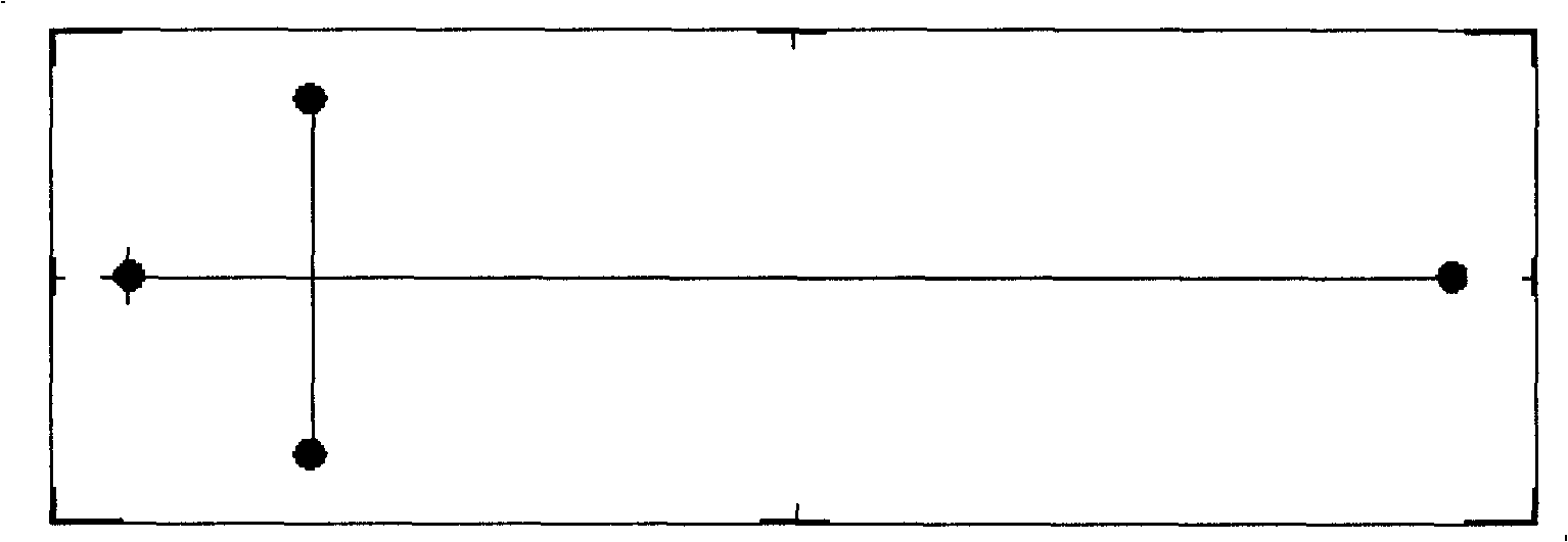
[0031] 1. Combine figure 1 , the shape of the middle channel is a simple straight channel form. Firstly, the plexiglass is processed into the required chip size (25*50mm 2 ), ultrasonically clean the surface with deionized water;

[0032] 2. Combine figure 2 , using a CNC milling machine to process straight channels, using the instrument on the chip 1 to control the lateral displacement on the X axis, the longitudinal displacement on the Y axis, and the scribe depth on the Z axis. The channel is 50 μm deep and 100 μm wide;

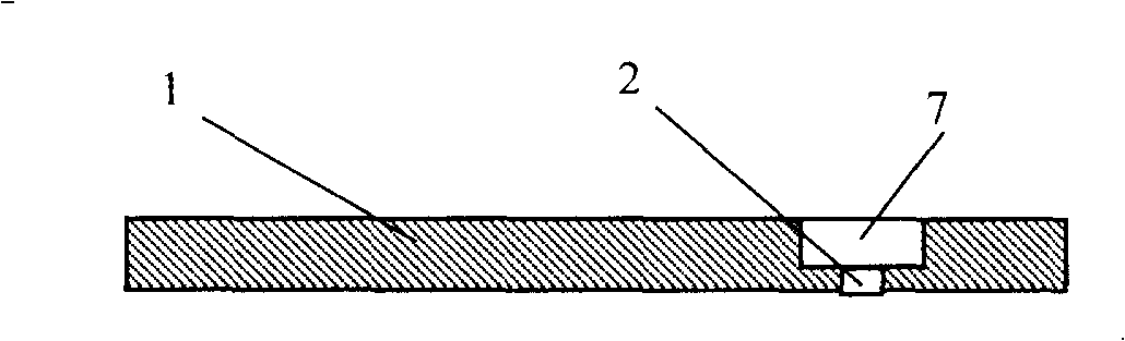
[0033] 3. After processing and manufacturing the channel, punch holes on the chip 1 as the sample pool, buffer sample pool, waste liquid pool, and sample recovery pool; and open the detection window 3 at the detection position for mounting slides and increasing absorption Optical path: First use a drill with a radius of 0.25mm to get through the test hole 2, and then use a milling cutter with a radius of 0.5mm to mill out 3×3mm 2 The square groove 7 ha...

Embodiment 2

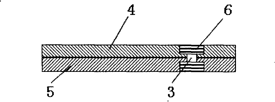
[0038] combine Figure 3-Figure 4 , the shape of the channel in this embodiment is a curved channel form with a curved corner shape, and the processing process is basically the same as in Example 1, only the channel scribing program is changed accordingly during the channel processing process.

[0039] 1. First process the plexiglass into the required chip size (30*30mm 2 ), ultrasonically clean the surface with deionized water;

[0040] 2. Use the CNC milling machine to process the curved groove, and control the turning radius and position of the groove through the corresponding program;

[0041] 3. After processing and manufacturing the channel, punch holes on the chip as the sample pool, buffer sample pool, waste liquid pool, and sample recovery pool; and open the detection window at the detection position to prepare for mounting slides and increase the absorption light path : First use a drill with a radius of 0.25mm to open it, and then use a milling cutter with a radiu...


PUM

PropertyMeasurementUnit
areaaaaaaaaaaa
widthaaaaaaaaaa
depthaaaaaaaaaa

Abstract

The invention proposes a preparation method for a micro-fluidic chip which is used for detecting ultraviolet - visible absorption, the structure of the chip is designed for biochemical analysis in an ultraviolet - visible absorption detection system. The structure of the micro-fluidic chip is used polymeric material such as synthetic glass (PMMA) as a substrate. A transmitted through-hole step structure is processed in a detection point position designed by the chip and glass which can pass through ultraviolet is implanted in a step position, then, problems that low transmission of ultraviolet light of the micro-fluidic chip in polymeric substrate and short optical length caused by a micron dimension groove. The chip of new type has simple structure, easy process, low cost technics, and is easy to popularize and apply.

Description

(1) Technical field [0001] The invention relates to the field of biochemical analysis, in particular to a structure of a microfluidic chip for ultraviolet-visible absorption detection. (2) Background technology [0002] As a commonly used test method in the field of biochemical analysis, ultraviolet-visible light absorption detection has relatively low detection sensitivity, but it has good versatility and can be directly measured; no special sample pretreatment process is required, the operation process is simplified, and the analysis efficiency is high; As a non-destructive detection method, it can be used in series with other detectors such as mass spectrometers, and has important application value in the field of biochemical analysis. However, its application in the field of microfluidic chip detection is limited because the materials used to make microfluidic chips are polydimethylsiloxane (PDMS), polymethyl methacrylate (PMMA), poly Carbonate (PC) is the main material...

Claims


Application Information

Patent Timeline
Patent Type & Authority Patents(China)
IPC IPC(8): G01N21/31G01N33/48G01N21/75G01N21/01
Inventor 刘晓为田丽王蔚张海峰李玲宋宇张业群
Owner HARBIN INST OF TECH
Why Eureka
Try Eureka