Method for improving illumination efficiency of organic electroluminescent device, and corresponding device thereof

A technology of light extraction efficiency and electroluminescence, applied in electroluminescence light source, electric solid device, electric light source, etc., can solve the problems of unutilized light energy and only light extraction efficiency of devices.

Inactive Publication Date: 2008-10-29
PEKING UNIV
View PDF0 Cites 13 Cited by
  • Summary
  • Abstract
  • Description
  • Claims
  • Application Information

AI Technical Summary

Problems solved by technology

So far, the light extraction efficiency of the device is still only 20% of the internal quantum efficiency, which means that about 80% of the light energy has not been utilized.

Method used


Image

  • Method for improving illumination efficiency of organic electroluminescent device, and corresponding device thereof
  • Method for improving illumination efficiency of organic electroluminescent device, and corresponding device thereof
  • Method for improving illumination efficiency of organic electroluminescent device, and corresponding device thereof

Examples


Embodiment 1

[0048] Embodiment 1. Fabrication and adjustment of device one (sapphire substrate / Au / white light device / Ag / Au)

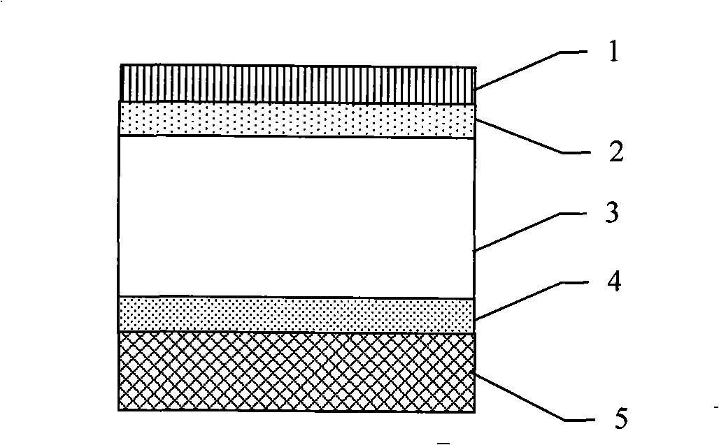
[0049] The cathode and anode of device 1 are both metal, and the manufacturing process is as follows: the substrate is sapphire (of course, other substrates can also be selected), and then a layer of gold is deposited as the anode by vacuum thermal evaporation; The traditional white light organic electroluminescent device (that is, the active layer) is produced by thermal evaporation; and then a layer of silver and gold are respectively deposited as a composite cathode by vacuum thermal evaporation.

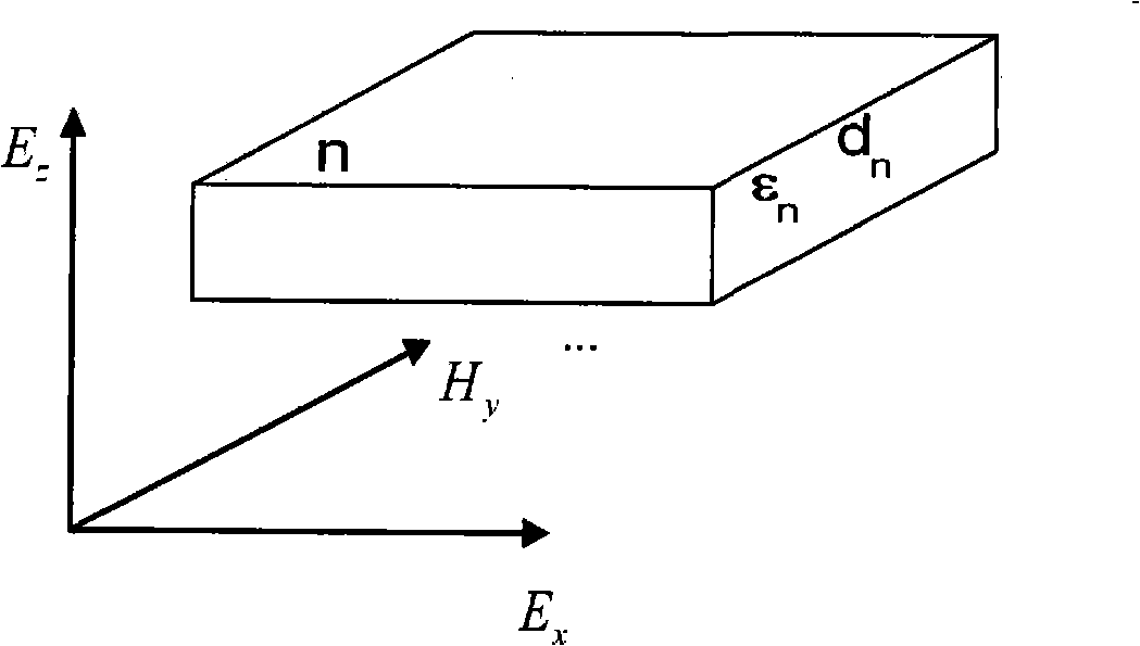
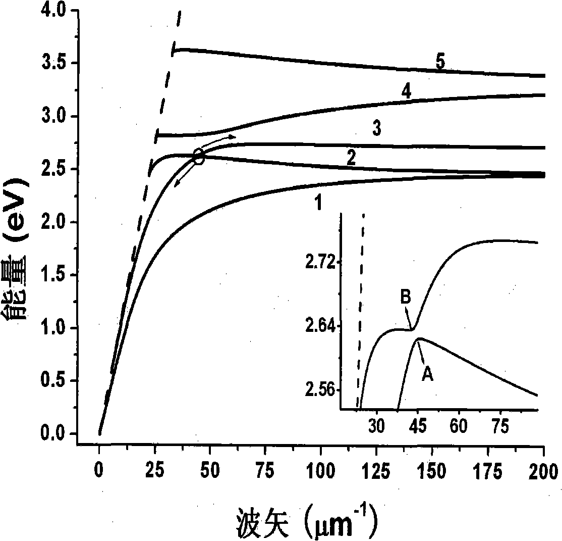
[0050] The device has five metal interfaces, so there are five surface plasmon dispersion branches. When the device parameters are: sapphire substrate / Au(20nm) / white light device (100nm) / Ag(10nm) / Au(10nm), get image 3 The surface plasmon dispersion curve is shown. image 3 The middle branches 1 and 2 are mainly determined by the metal anode, and the branches 3, 4 an...

Embodiment 2

[0051] Embodiment 2. Fabrication and adjustment of device two (sapphire substrate / Au / white light device / Ag / Au / GaP)

[0052] On the basis of device one, a cap layer is deposited on the composite cathode by sputtering to obtain device two. When the cap layer material is gallium phosphide (ε=12.4), and the thickness of each layer of the device is sapphire substrate / Au(10nm) / white light device (100nm) / Ag(20nm) / Au(10nm) / GaP(10nm), the device The surface plasmon dispersion curve of the second is as Figure 5 shown. Due to the addition of a high dielectric constant cap layer on the composite cathode silver and gold, the 3-branch of the cathode is depressed to the anti-cross coupling with the 1-branch of the anode. Depend on Figure 5 It can be seen that the wave vector of the two is about 79.18 μm -1 place where anti-cross-coupling occurs (see Figure 5 The partially enlarged inset in the lower right corner), the energy of this resonant plasmonic channel is 2.06 eV. By adjustin...

Embodiment 3

[0053] Embodiment 3. Fabrication and adjustment of device three (Si substrate / white light device / Ag / Au / GaP)

[0054] This example shows the operation of a device where only one electrode is metallic. At this time, the position of the luminescent excitons is required to be relatively close to the cathode.

[0055] When the position of the luminescent excitons is relatively close to the cathode (within 20nm), we can simply adjust the thickness of the cap layer above the cathode to achieve the transmission from red light to blue light.

[0056] Device manufacturing process: the substrate is selected as a silicon chip so as to be integrated with the existing silicon technology, and silicon also serves as an anode. Then use spin coating or vacuum thermal evaporation to fabricate traditional white light organic electroluminescent devices, then use thermal evaporation to deposit a layer of silver and gold as a composite cathode, and finally deposit a layer of silver on the cathode b...


PUM


Abstract

The invention provides a method for improving extraction efficiency of an organic electroluminescent (EL) device. By adopting the inherent surface plasmon waves of devices with metal electrodes as media, a surface plasmon tunnel energy resonating with the light emitting exciton is formed by adjusting parameters of the device, namely, changing the dielectric constant and thickness of materials on each layer. Introduce the energy of light emitting exciton to the tunnel, and then release the energy in the tunnel through micro-nano structure of the device, thus avoiding light energy waste caused by consumption of light energy resulted from useless waveguide mode and other modes and improving the extraction efficiency of the device. The invention also provides an organic EL device working according to the principle. Transmission of various colors of lights from blue to red can be realized by adjusting parameters of the device, thus replacing the practice of arranging a color filter in front of a white light source in traditional organic EL display technology.

Description

technical field [0001] The invention relates to an organic electroluminescence (EL) device and belongs to the technical field of organic electroluminescence display. technical background [0002] Organic electroluminescent display is currently recognized as a promising flat-panel display technology in the world. It has many advantages: (1) it uses organic matter and has a wide range of material choices, which can display any color from blue light to red light; ( 2) The driving voltage is low, which can match the driving voltage of the integrated circuit; (3) The luminous brightness is high; (4) Fully cured active light; (5) The viewing angle is wide, up to 160 degrees, and the response speed is fast, which is 1000 degrees of liquid crystal. (6) simple preparation and low cost; (7) ultra-thin film, light in weight; (8) low energy consumption, excellent low temperature and shock resistance; (9) can be made into a soft screen display. [0003] The most common structure of orga...

Claims


Application Information

Patent Timeline
Patent Type & Authority Applications(China)
IPC IPC(8): H01L51/50H05B33/12
Inventor 陈志坚兰智豪王紫瑶龚旗煌
Owner PEKING UNIV
Why Eureka
Try Eureka