Method for preparing single crystal zinc blende nano-wire

A technology of nanowires and zinc sulfide, applied in the field of preparation of zinc sulfide nanowires, can solve the problems affecting the physical properties of ZnS nanostructures and the high synthesis temperature, and achieve the effects of easy large-scale production, easy availability of raw materials and low cost.

Inactive Publication Date: 2008-11-26
UNIV OF SCI & TECH BEIJING
View PDF0 Cites 2 Cited by
  • Summary
  • Abstract
  • Description
  • Claims
  • Application Information

AI Technical Summary

Problems solved by technology

However, in their reports, the synthesis temperature of ZnS nanomaterials is relatively high (1000-1200 °...

Method used


Image

  • Method for preparing single crystal zinc blende nano-wire

Examples


Embodiment 1

[0018] 1. Ultrasonic cleaning the blank silicon wafer in alcohol and acetone respectively;

[0019] 2. In the tube furnace, feed a flow rate of argon and hydrogen gas mixture (the volume ratio of hydrogen and argon is 10: 100);

[0020] 3. Put the ZnS powder in a quartz boat as an evaporation source, and put it in a tube furnace together with the boat. The cleaned silicon wafer is also placed in the furnace, 30mm away from the evaporation source, wherein the evaporation source is placed upstream of the incoming airflow, and the silicon wafer is placed downstream of the airflow;

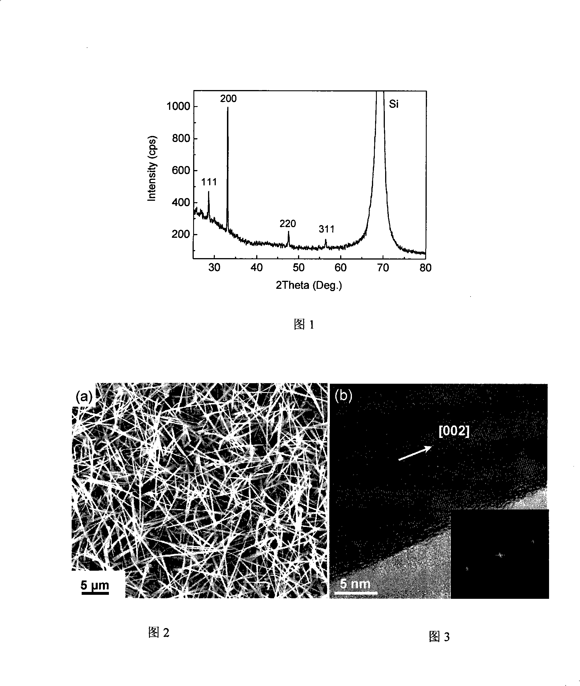
[0021] 4. Heat up the temperature of the tube furnace to 900°C, and the holding time is 100min. The pressure in the furnace is 0.015MPa. After the temperature of the furnace dropped to room temperature, the silicon wafer was taken out, and a layer of ZnS nanowire white film was deposited on the silicon wafer.

[0022] Figure 1 is the X-ray diffraction pattern of the product, and all diffraction pea...

Embodiment 2

[0024] 1. Ultrasonic cleaning the blank silicon wafer in alcohol and acetone respectively;

[0025] 2. In the tube furnace, feed a flow rate into a mixture of argon and hydrogen (the volume ratio of hydrogen and argon is 13: 100);

[0026] 3. Put the ZnS powder in a quartz boat as an evaporation source, and put it in a tube furnace together with the boat. The cleaned silicon wafer is also placed in the furnace, 25mm away from the evaporation source, wherein the evaporation source is placed upstream of the incoming airflow, and the silicon wafer is placed downstream of the airflow;

[0027] 4. The temperature of the tube furnace was raised to 890° C., and the holding time was 120 minutes. The pressure in the furnace is 0.03MPa. After the temperature of the furnace dropped to room temperature, the silicon wafer was taken out, and a layer of ZnS nanowire white film was deposited on the silicon wafer.

Embodiment 3

[0029] 1. Ultrasonic cleaning the blank silicon wafer in alcohol and acetone respectively;

[0030] 2. In the tube furnace, the mixed gas of argon and hydrogen (the volume ratio of hydrogen and argon is 8: 100) is fed into the flow rate of 108ml / min;

[0031] 3. Put the ZnS powder in a quartz boat as an evaporation source, and put it in a tube furnace together with the boat. The cleaned silicon wafer is also placed in the furnace, 28mm away from the evaporation source, wherein the evaporation source is placed upstream of the incoming airflow, and the silicon wafer is placed downstream of the airflow;

[0032] 4. The temperature of the tube furnace was raised to 910°C, and the holding time was 80 minutes. The pressure in the furnace is 0.025MPa. After the temperature of the furnace dropped to room temperature, the silicon wafer was taken out, and a layer of ZnS nanowire white film was deposited on the silicon wafer.


PUM

PropertyMeasurementUnit
Diameteraaaaaaaaaa
Tip diameteraaaaaaaaaa
Lengthaaaaaaaaaa

Abstract

The invention relates to a preparation method of a single crystal ZnS nano-wire, which belongs to the field of preparative technique of semiconductor material. The method comprises the following steps: inletting the mixed gas of argon and hydrogen with a flow rate of 108 to 113ml/min into a tube furnace; putting the ZnS powder in a quartz boat as a evaporation source, and putting the ZnS powder together with the boat in the tube furnace, and putting a cleaned silicon chip in the furnace, which is 25 to 30mm from the evaporation source, wherein the evaporation source is in the direction of inlet airflow while and the silicon chip is in the direction of outlet airflow; heating the tube furnace to 890 to 910 DEG C with the holding time of 80 to 120min and a pressure of 0.015 to 0.03MPa in the furnace. A layer of white ZnS nano-wire film is deposited on the silicon chip when the temperature of the furnace drops to a room temperature. The method requires a low synthesis temperature and does not apply a foreign catalyst. The prepared ZnS nano-wire has a face-centered cubic structure; the length of 10 to 15Mum and a diameter of only 20 to 30nm at the tip. The nano-wire is single crystal with a higher crystalline quality. The preparation method has the advantages of simple and convenient operating process, available raw material, low cost and easy scale production.

Description

technical field [0001] The invention belongs to the technical field of semiconductor material preparation, and relates to a preparation method of zinc sulfide nanowires. Background technique [0002] Semiconductor nanomaterials have potential applications in optics, electricity, magnetism, and nanoelectronics, and are one of the research hotspots in nanomaterials science in recent years. With the nanometerization of semiconductor materials, it can not only cause the blue shift of absorption wavelength and fluorescence emission, but also produce nonlinear optical effects, and enhance the redox ability of nanomaterials, which has more excellent photocatalytic activity. Zinc sulfide (ZnS) is an important II-VI group direct bandgap semiconductor with a forbidden band width of 3.6-3.8eV. It has piezoelectricity, pyroelectricity, infrared transparency and good luminescence properties. It has been widely studied as a material. It has a wide range of applications in many fields suc...

Claims


Application Information

Patent Timeline
IPC IPC(8): C30B29/48C30B29/62C30B23/00
Inventor 常永勤
Owner UNIV OF SCI & TECH BEIJING
Why Eureka
Try Eureka