Solar spectrum selective absorption film and preparation method thereof
A solar spectrum and selective technology, applied in the field of solar spectrum selective absorption film, can solve the problems of unsatisfactory absorption ratio and emissivity performance, high power consumption, long sputtering time, etc., and achieve air-drying performance improvement, The effect of stable thermal performance and low price
- Summary
- Abstract
- Description
- Claims
- Application Information
AI Technical Summary
Problems solved by technology
Method used
Image
Examples
Embodiment 1
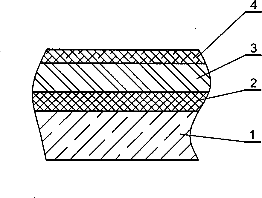
[0019] A solar spectrum selective absorption film, comprising a coating substrate, on the surface of the substrate, an infrared reflection layer, an absorption layer, and an anti-reflection layer are sequentially covered from the inside to the outside; the infrared reflection layer contains titanium elements + aluminum elements + a sputtering deposition layer (Ti+Al+Si) of silicon element, the absorbing layer is a sputtering deposition layer comprising aluminum-nitrogen clusters + titanium-nitrogen clusters + silicon-nitrogen clusters + aluminum-titanium-silicon clusters ( AlN+TiN+Si 3 N 4 +AlTiSi); the anti-reflection layer is a sputtering deposition layer (AlN+TiN+Si 3 N 4 ). see figure 1 , the coating substrate is a plane heat-absorbing plate 1, on which the infrared reflection layer 2, the absorption layer 3, and the anti-reflection layer 4 are sequentially covered from the inside to the outside; the thickness of the infrared reflection layer is 70 to 90 nanometers (nm...
Embodiment 2
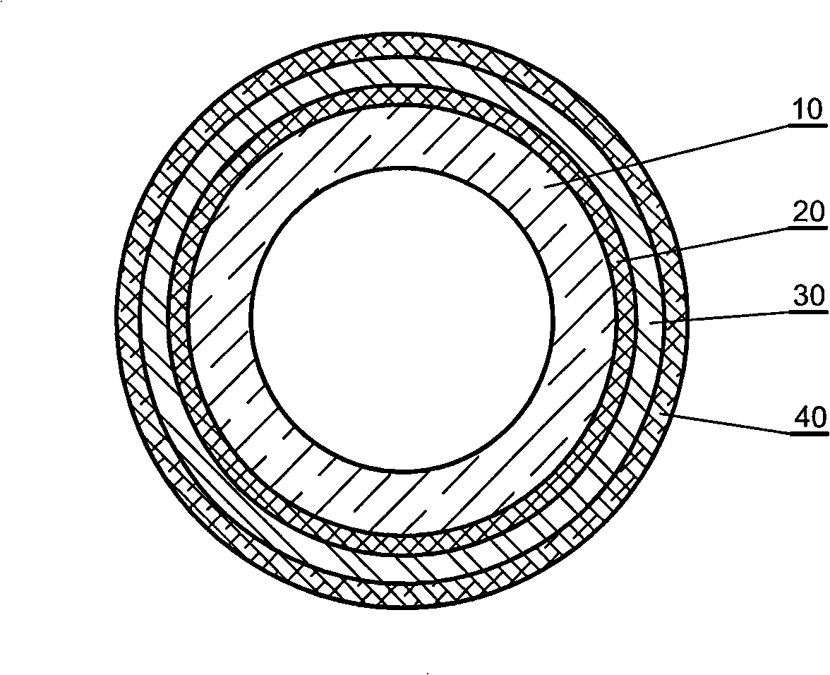
[0021] see figure 2 , the film-coated substrate of the present invention is a glass inner tube 10 in a solar vacuum heat collecting tube, figure 2 It is a cross-sectional view of the glass inner tube, showing only the glass inner tube and coating structure, not the glass outer tube. The outer surface of the glass inner tube is covered with an infrared reflection layer 20, an absorption layer 30, an anti-reflection layer, and Layer 40; in the present embodiment, the thickness of the infrared reflective layer is 70-90 nanometers, the optimum thickness is 90 nanometers; the thickness of the absorption layer is 70-90 nanometers, the optimum thickness is 80 nanometers; The thickness of the anti-reflection layer is 40-60 nanometers, and the optimum thickness is 40 nanometers.
[0022] In the present embodiment, the experimental data of using the glass inner tube coated with the method of the present invention and the glass inner tube of the common heat collecting tube are as foll...
Embodiment 3
[0027] A kind of preparation method of solar spectrum selective absorption film, the magnetron sputtering coating device used in the present embodiment is the 850 type magnetron sputtering coating machine that Hunan Hengyang produces, and the used nitrogen stable amount when applying this equipment is 55SCCM (SCCM-the number of milliliters of gas flowing in per minute under the standard state). The film-coated substrate is the glass inner tube in the solar vacuum heat collecting tube. In other embodiments, the film-coated substrate can also be a metal pipe, a metal plate or a glass plate.
[0028] Its operation steps are:
[0029] A, the coating substrate is installed in the coating chamber of the magnetron sputtering coating device, the vacuum in the coating chamber is set to 0.0065Pa, and the magnetron sputtering coating machine includes a titanium-silicon alloy target, an aluminum alloy target (its model It is domestic LY11-13); the vacuum degree can also be expressed as ...
PUM
| Property | Measurement | Unit |
|---|---|---|
| Thickness | aaaaa | aaaaa |
| Thickness | aaaaa | aaaaa |
| Thickness | aaaaa | aaaaa |
Abstract
Description
Claims
Application Information


