Method for manufacturing silicon single crystal wafer
A manufacturing method and technology of single crystal silicon, applied in the direction of single crystal growth, single crystal growth, chemical instruments and methods, etc., can solve problems such as low component characteristics
- Summary
- Abstract
- Description
- Claims
- Application Information
AI Technical Summary
Problems solved by technology
Method used
Image

Examples
Embodiment 1
[0093] Embodiment 1, comparative example 1
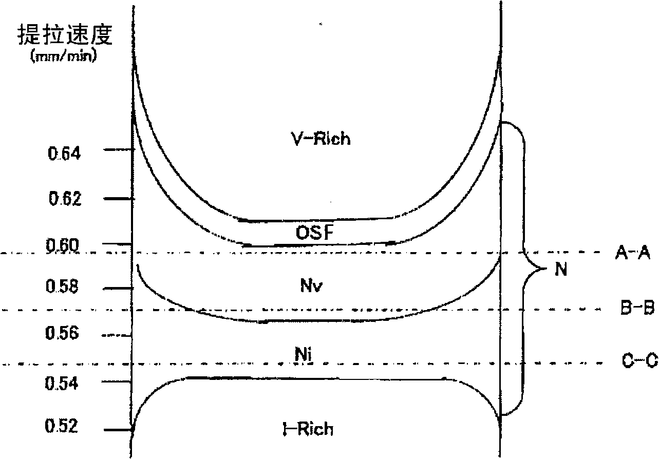
[0094] Using the same single crystal pulling device as conventionally used, growth of silicon single crystal wafers was performed by continuously reducing the pulling speed from 0.7 mm / min to 0.5 mm / min while controlling the diameter to 210 mm.
[0095] In this case, the defect distribution of the cross-section of the ingot parallel to the pulling axis is as figure 1 shown.
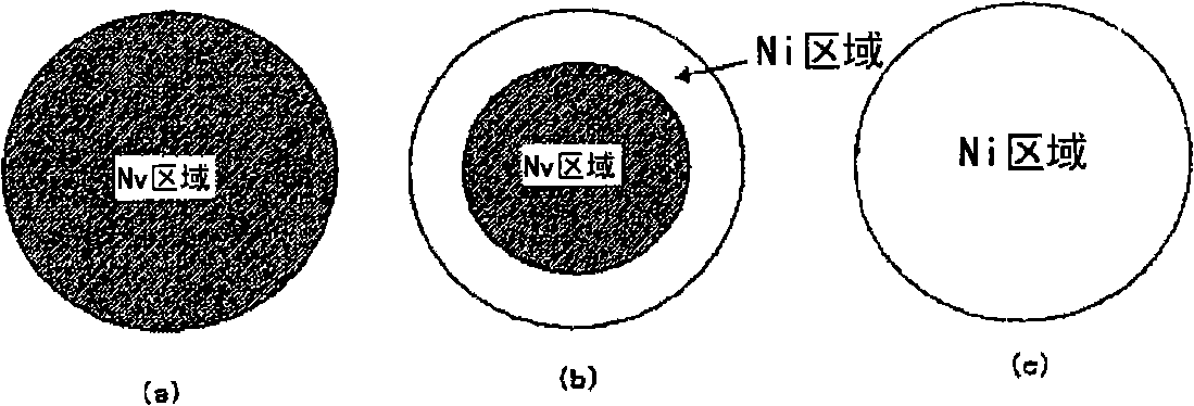
[0096] Therefore, using the single crystal pulling device in the same hot zone, the pulling speed is 0.595mm / min ( figure 1 A-A position) mode, pulling the monocrystalline silicon ingot while controlling it, to prepare the wafer cut out in the radial direction. The defect distribution of this wafer is as follows figure 2 As shown in (a), the entire surface (the entire surface) is an Nv region (hereinafter referred to as an Nv wafer).
[0097] Again, with the pulling speed as 0.57mm / min ( figure 1 B-B position) mode, pulling the monocrystalline silicon ing...
Embodiment 2
[0117] Embodiment 2, comparative example 2
[0118] Next, use the single crystal pulling device in the same hot zone as the pulling device used in Example 1, with a pulling speed of 0.595 mm / min ( figure 1 The A-A position) method, while controlling and pulling the monocrystalline silicon ingot, to prepare the Nv wafer cut out in the radial direction, for the Nv wafer, in the NH 3 In a mixed environment with a flow rate of 0.5L / min and an Ar flow rate of 4L / min, the temperature was rapidly raised from room temperature at a heating rate of 50°C / s, kept at 1200°C for 10 seconds, and then rapidly cooled at a cooling rate of 50°C / s. After that, at N 2 Under ambient conditions, heat treatment was performed by changing the heat treatment temperature (700°C, 800°C, 900°C) and heat treatment time (10 minutes, 30 minutes, 60 minutes), and then the oxide film withstand voltage was measured for each wafer.
[0119] As a result, in Figure 7 , and Table 2 show the relationship between ...
PUM
 Abstract
Description
Claims
Application Information
 - R&D
- Intellectual Property
- Life Sciences
- Materials
- Tech Scout
- Unparalleled Data Quality
- Higher Quality Content
- 60% Fewer Hallucinations
Browse by: Latest US Patents, China's latest patents, Technical Efficacy Thesaurus, Application Domain, Technology Topic, Popular Technical Reports.
© 2025 PatSnap. All rights reserved.Legal|Privacy policy|Modern Slavery Act Transparency Statement|Sitemap|About US| Contact US: help@patsnap.com