
Flip-attached and underfilled stacked semiconductor devices

A semiconductor and substrate technology, applied in the direction of semiconductor devices, semiconductor/solid-state device manufacturing, semiconductor/solid-state device components, etc., can solve the problems of chip passivation layer cracks, solder joint delamination, crack propagation circuit structure, etc., to achieve The effect of reducing thermomechanical stress, increasing throughput, and simplifying process flow

Inactive Publication Date: 2009-02-18
TEXAS INSTR INC
View PDF0 Cites 5 Cited by
  • Summary
  • Abstract
  • Description
  • Claims
  • Application Information

AI Technical Summary

Problems solved by technology

The stresses created by these process steps can cause delamination of the solder joints, crack the passivation layer of the chip, or propagate cracks into the circuit structure

Method used


Image

  • Flip-attached and underfilled stacked semiconductor devices
  • Flip-attached and underfilled stacked semiconductor devices
  • Flip-attached and underfilled stacked semiconductor devices

Examples


Embodiment Construction

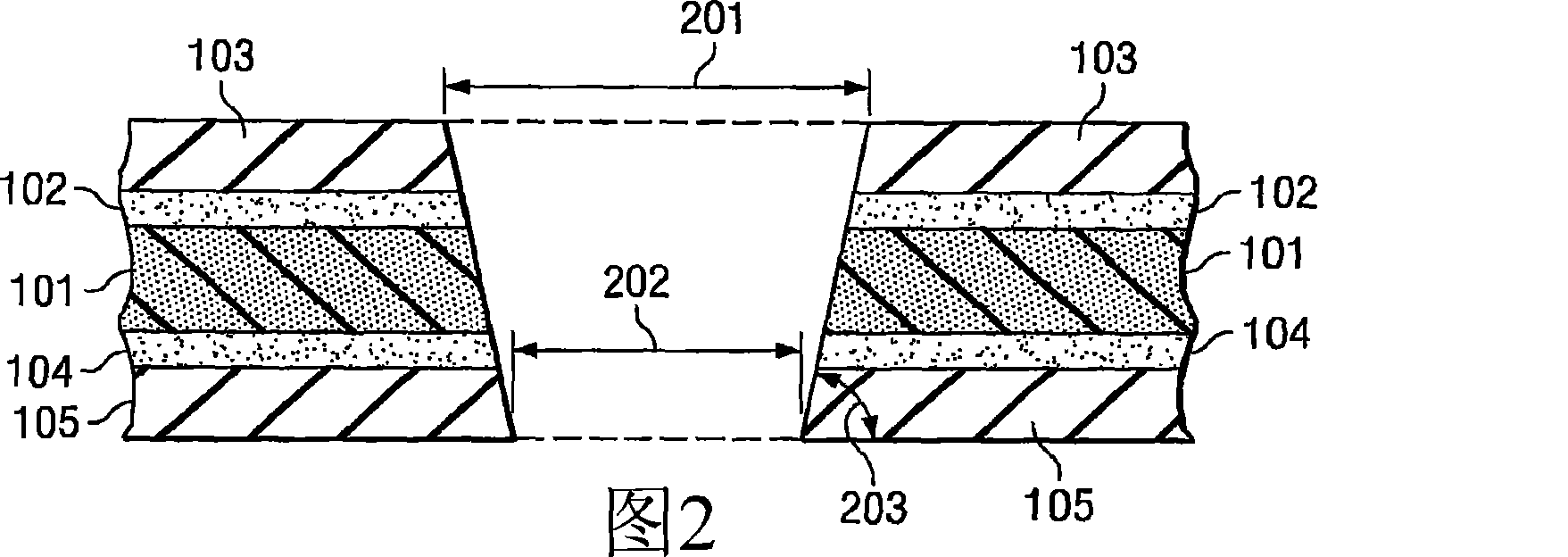
[0023] exist Figure 1A One embodiment of the present invention is depicted in a schematic cross-section of a strip (generally indicated as 100 ), which is used as a carrier and especially in a semiconductor device assembly. The strip 100 consists of a base plate 101 of polymeric material, preferably thermoplastic, having a thickness ranging from about 25 to 450 μm; for some devices said thickness can reach about 800 μm. Preferred thermoplastic chassis materials include: long chain polyimide plus acrylic or silicone, long chain polyethylene plus acrylic, and long chain polypropylene plus acrylic. Preferably, the backplane material is chosen such that it softens and enters a low viscosity or liquid phase in the same temperature range required to reflow components embedded in tape (see below). For example, this temperature range includes the melting temperature of the solder selected for assembling the device. A technical advantage is that, when the base plate is chosen from th...


PUM


Abstract

The invention discloses a tape for use as a carrier in semiconductor assembly, which has one or more base sheets (101) of polymeric, preferably thermoplastic, material having first (101a) and second (101b) surfaces. A polymeric adhesive film (102, 104) and a foil (103, 105) of different, preferably inert, material are attached to the base sheet on both the first and second surface sides; they thus provide a thickness (120) to the tape. A plurality of holes is formed through the thickness of the tape; the holes are preferably tapered with an angle between about 70 DEG and 80 DEG with the second tape surface. A reflow metal element (301), with a preferred diameter (302) about equal to the tape thickness, is held in each of the holes.

Description

technical field [0001] The present invention relates generally to the fields of electronic systems and semiconductor devices; and more particularly to the fabrication of flip-chip mounted, underfilled and stacked semiconductor devices. Background technique [0002] When an integrated circuit (IC) chip is mounted on an insulating substrate (such as a printed circuit motherboard) with wires using solder bump connections, the chip is separated from the substrate by a gap; the solder bump interconnects extending across the gap. The IC chip is usually a semiconductor such as silicon, silicon germanium or gallium arsenide and the substrate is often made of a ceramic or polymer based material such as FR-4. Therefore, there is a significant difference between the coefficient of thermal expansion (CTE) of the chip and the substrate; for example, between silicon (approx. In the case of materials, the difference in CTE is about an order of magnitude. As a result of this CTE differen...

Claims


Application Information

Patent Timeline
Patent Type & Authority Applications(China)
IPC IPC(8): H01L23/29
CPCH01L2924/10329H01L2924/01027H05K2201/10424H05K3/3436H01L24/29H01L25/105H01L2224/81801H01L2224/8388H01L24/12H01L2224/83101H05K2203/0191H01L2924/01015H01L2924/01032H01L2924/01087H05K2203/043H01L23/4985H01L2224/48091H01L2224/81101H01L23/49816H01L2924/01004H01L2924/01006H01L21/6835H01L2224/73203H05K2201/10977H01L24/48H01L24/16H01L24/11H01L2924/14H05K2203/041H01L2924/10253H01L2924/01005H01L2224/11334H01L2225/1023H01L2924/01082H01L2224/13099H01L21/563H01L2924/014H05K3/3478H01L2225/1058H01L2224/48227H01L2924/01033H01L2924/01075H01L24/81H01L2224/11474H01L2224/1148H01L2924/00014H01L2924/15787H01L2924/181Y02P70/50H01L2924/3512H01L2924/00H01L2224/45099H01L2224/45015H01L2924/207H01L23/48
Inventor 天谷正纯渡边雅子
Owner TEXAS INSTR INC
Learn More