
Method for preparing nano-scale pattern substrate for nitride epitaxial growth

An epitaxial growth, patterned substrate technology, applied in semiconductor/solid-state device manufacturing, electrical components, circuits, etc., can solve the problems of large area, large-scale production, expensive equipment, complex process, etc. The effect of large area production and reduced production cost

Inactive Publication Date: 2009-02-25
UNILUMIN GRP
View PDF0 Cites 59 Cited by
  • Summary
  • Abstract
  • Description
  • Claims
  • Application Information

AI Technical Summary

Problems solved by technology

[0005] The realization of semiconductor nanoscale patterns usually adopts electron beam lithography or X-ray lithography, but these lithography involve expensive equipment, complicated process and high cost, and cannot be large-scale and large-scale make

Method used


Image

  • Method for preparing nano-scale pattern substrate for nitride epitaxial growth
  • Method for preparing nano-scale pattern substrate for nitride epitaxial growth
  • Method for preparing nano-scale pattern substrate for nitride epitaxial growth

Examples


Embodiment 1

[0052] This embodiment is a method for fabricating a nanoscale patterned sapphire substrate for nitride epitaxial growth. Sapphire substrate is one of the most commonly used substrate materials for epitaxial nitride growth.

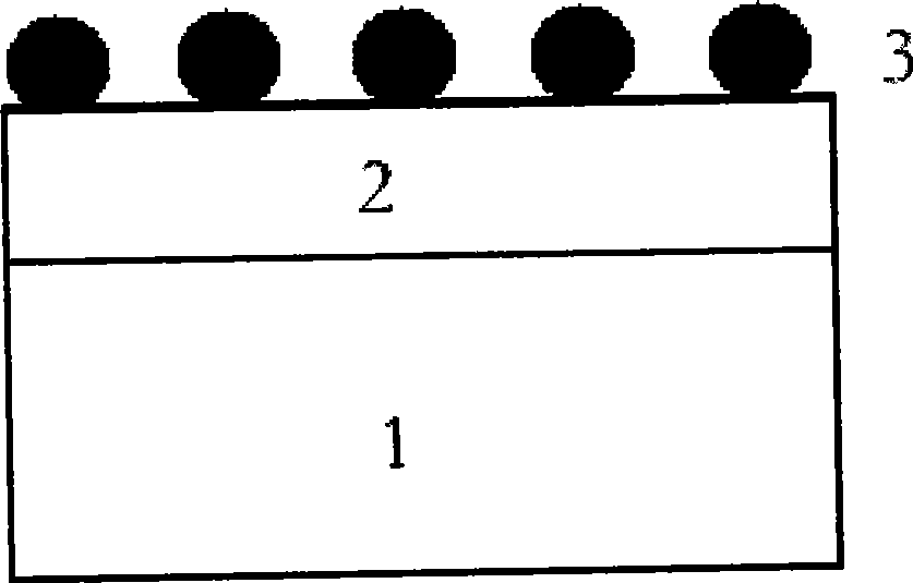
[0053] First, a 0.5-micron silicon dioxide film is deposited on a 2-inch sapphire substrate by plasma-enhanced chemical vapor deposition (PECVD), and then a 15-nm nickel metal layer is evaporated by electron beam evaporation. The structure profile is as follows: figure 2 shown;

[0054] Then in the flowing N 2 , and annealed at 850 degrees for 5 minutes to form nanoscale nickel metal particles on the surface. The structure profile is as follows image 3 shown;

[0055] Then use nano-scale nickel metal particles as a mask, and use RIE or ICP plasma etching equipment to dry-etch the silicon dioxide film to form a nano-pattern structure. The scale of the pattern is about 50-150nm, and the structure profile is Figure 4 shown;

[0056] Then use the sili...

Embodiment 2

[0059] This embodiment is a method for fabricating a nanoscale patterned Si(111) substrate for nitride epitaxial growth. Si(111) substrate is one of the commonly used substrate materials for epitaxial nitride growth.

[0060] First, a 0.5 micron silicon nitride film is deposited on a Si(111) substrate by PECVD technology and a 15nm titanium (Ti) metal thin layer is evaporated by electron beam method. The structure profile is as follows: figure 2 shown;

[0061] Then in the flowing N 2 Annealing at 950°C for 20 minutes to form nanoscale titanium (Ti) metal particles with a structural profile such as image 3 shown;

[0062] Then use nanometer-scale metal titanium (Ti) particles as a mask, and use RIE or ICP equipment to dry-etch the silicon nitride film to form a nano-graphic structure. The graphic scale is about 100-300nm, and the structural section is as follows Figure 4 shown;

[0063] Then use the silicon nitride film of the nano-pattern structure as a mask, and use ...


PUM

PropertyMeasurementUnit
thicknessaaaaaaaaaa
thicknessaaaaaaaaaa
thicknessaaaaaaaaaa

Abstract

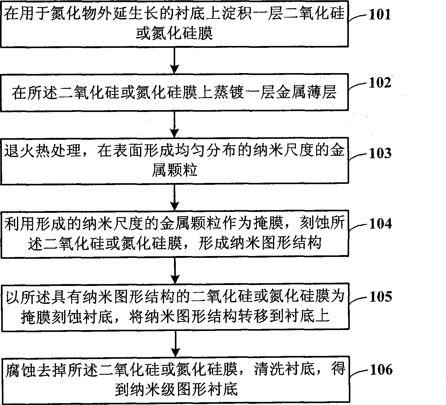
The invention relates to the semiconductor technical field and discloses a method for manufacturing a nanometer pattern substrate used for the epitaxial growth of a nitride. The method comprises the followings steps: settling a layer of silicon dioxide or silicon nitride film on a substrate used for the epitaxial growth of the nitride; the silicon dioxide or silicon nitride film is coated with a layer of thin metal layer through vapor deposition; conducting the annealing heat treatment, and forming uniformly distributed nano-scaled metal particles; utilizing the formed nano-scaled metal particles as masks to etch the silicon dioxide or silicon nitride film so as to form a nanometer pattern structure; using the silicon dioxide or silicon nitride film with the nanometer pattern structure as a mask etching substrate to transfer the nanometer pattern structure of the substrate; and etching to remove the silicon dioxide or silicon nitride film, cleaning the substrate, and obtaining the nanometer pattern substrate. The invention can reduce the dislocation density in the epitaxial layer of the nitride, improve the crystal quality of epitaxial materials, improve the performance of devices and help to realize the scaled and large area manufacture.

Description

technical field [0001] The invention relates to the technical field of semiconductors, in particular to a method for manufacturing a nanoscale pattern substrate used for nitride epitaxial growth. Background technique [0002] Wide-bandgap nitride compound semiconductors represented by III-V gallium nitride (GaN) are used in ultraviolet / blue / green light-emitting diodes, lasers, solar-blind ultraviolet photodetectors, and high-frequency, high-temperature, high-power electronics Devices and many other aspects have important and extensive applications. Nitride is mainly heteroepitaxially grown on sapphire, silicon, silicon carbide, zinc oxide, gallium arsenide substrates, or homoepitaxially grown on free-standing gallium nitride substrates. [0003] Except for free-standing GaN substrates, there are large lattice constant mismatches and differences in thermal expansion coefficients between other substrates and nitrides. Therefore, in the nitride epitaxial layer grown by metal-...

Claims


Application Information

Patent Timeline
Patent Type & Authority Applications(China)
IPC IPC(8): H01L21/308
Inventor 闫发旺高海永樊中朝李晋闽曾一平王国宏张会肖王军喜张扬
Owner UNILUMIN GRP
Learn More