Manufacturing and repairing method for conductive circuit of three dimensional mold interconnecting device

A technology for molding interconnection and conductive lines, which is used in printed circuit manufacturing, printed circuit, conductive pattern formation, etc. Material cost reduction, low cost effect

Active Publication Date: 2009-03-25
WUHAN XINRUIDA LASER ENG
View PDF1 Cites 38 Cited by
  • Summary
  • Abstract
  • Description
  • Claims
  • Application Information

AI Technical Summary

Problems solved by technology

Some large integrated parts can be produced through injection compounding, such as door panels and center pillars of automobiles, but due to the processing method, the three-dimensional structure design is limited and cannot be used to produce products with complex structures
[0007] With the development of plastic electronic products in the direction of miniaturization, light weight, high density, low cost, small batch, diversification, and environmental protection, there are some deficiencies in the above 3D-MID manufacturing technology: first, it is moldable with plating The base material of structural parts is expensive. For example, in order to obtain platable plastics, the secondary two-component injection method often adds precious metals such as palladium (Pd) and gold (Au) to the plastics to obtain the so-called catalytically activated platable plasti...

Method used


Image

  • Manufacturing and repairing method for conductive circuit of three dimensional mold interconnecting device
  • Manufacturing and repairing method for conductive circuit of three dimensional mold interconnecting device

Examples


Embodiment 1

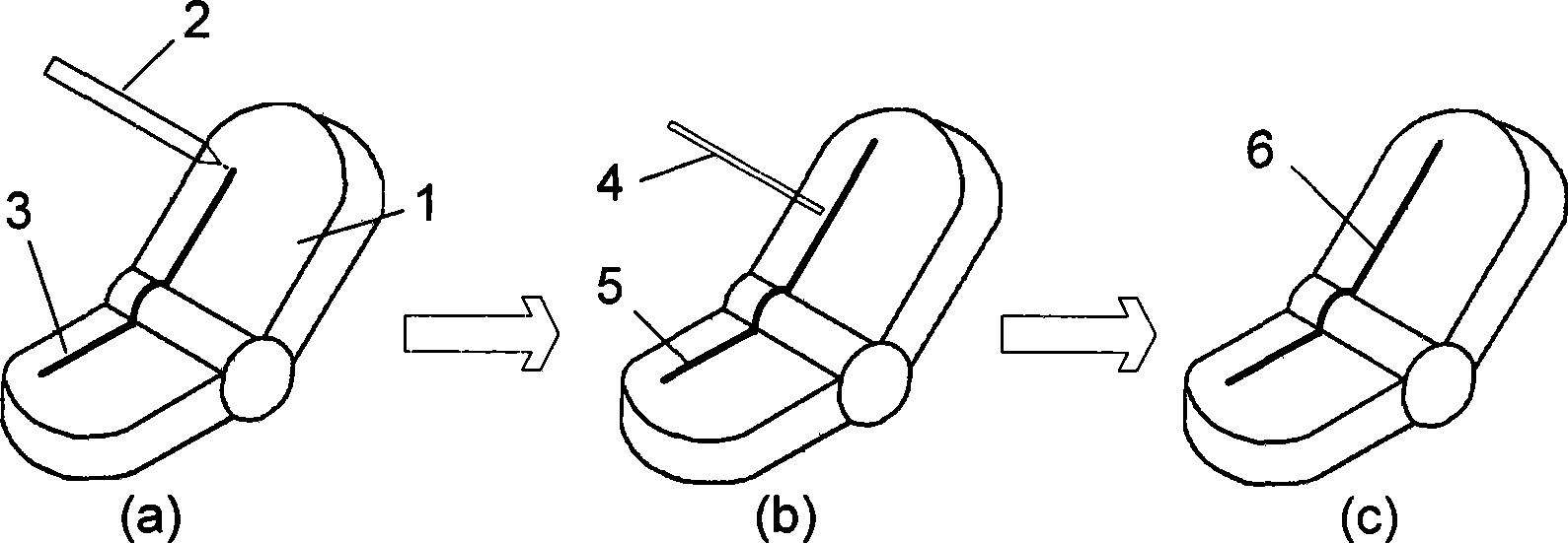
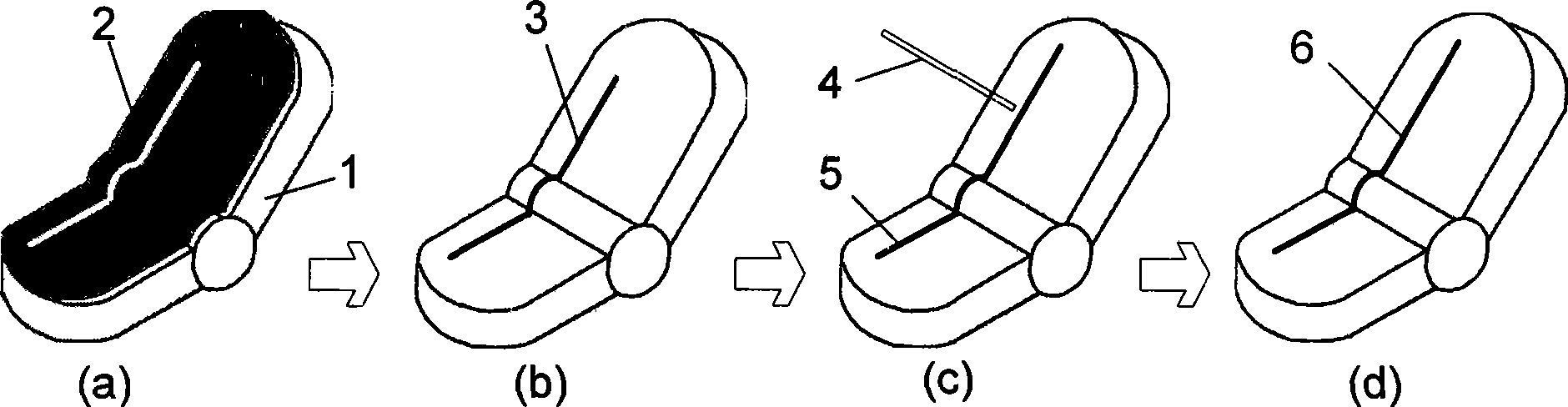
[0042] The molded structural parts used in this embodiment are made of polystyrene (PS) and formed by compression molding, and the conductive paste used is gold-based paste. First, using the micro-pen direct writing deposition process, according to the spatial trajectory of the conductive path designed and generated by CAD software, the conductive paste is preset on the molded structural parts to form a preset paste layer of about 10 microns, and dried at 90°C for 30 minutes to remove organic solvents. Then, use a continuous Nd:YAG laser with a maximum output power of 50W to scan and irradiate the dried preset slurry layer according to the conductive path space trajectory designed and generated by CAD software, with a scanning speed of 10mm / s and a single scanning line The width is 100 microns, and the wider pre-set slurry layer is scanned by multiple laps. Thereafter, electroless copper plating and nickel plating are performed sequentially according to the standard process, ...

Embodiment 2

[0044] The molded structural part used in this embodiment is made of liquid crystal polymer (LCP) material, which is formed by injection molding process, and the conductive paste used is gold-based paste. First, using the micro-nozzle direct writing deposition process, the conductive paste is preset on the molded structural parts into a preset paste layer of about 5 microns according to the spatial trajectory of the conductive path designed and generated by the CAD software, and dried at 85°C for 30 minutes to remove the organic solvent. Then, using a continuous CO with a maximum output power of 100W 2 The laser also scans the dried preset slurry layer according to the conductive path space trajectory designed and generated by the CAD software. The scanning speed is 25mm / s, and the single scan line width is 120 microns. The wider preset slurry layer is The scanning is completed by multi-pass overlapping. After that, electroless copper plating and nickel plating are carried ou...

Embodiment 3

[0046] The molded structural parts used in this embodiment are made of polyethylene (PE) and formed by compression molding process, and the conductive paste used is copper-based paste. First, using the micro-nozzle direct writing deposition process, the conductive paste is preset on the molded structural parts into a preset paste layer of about 10 microns according to the spatial trajectory of the conductive path designed and generated by the CAD software, and dried at 80°C for 40 minutes to remove the organic solvent. Then, use a continuous Nd:YAG laser with a maximum output power of 50W to scan the dried preset slurry layer according to the conductive path space trajectory designed and generated by the CAD software. The scanning speed is 15mm / s, and the single-scanning linewidth 100 microns, and the wider preset slurry layer is scanned by multiple laps. After that, electroless copper plating and chrome plating are performed sequentially according to the standard process, and...


PUM

PropertyMeasurementUnit
Thicknessaaaaaaaaaa
Thicknessaaaaaaaaaa
Thicknessaaaaaaaaaa

Abstract

The invention discloses a method for manufacturing and repairing a three-dimensional molding interconnection device conductive line. The method comprises the following steps: (1) depositing a 0.1-50 micrometer thick prearranged sizing agent layer of a conductive sizing agent on the surface of a molding structural element according to the design configuration of a conductive line; (2) baking or airing the prearranged layer of the conductive sizing agent, and removing an organic solvent thereof; (3) utilizing a laser beam to irradiate the prearranged sizing agent layer so as to enable metal conductive particles in the sizing agent to be melted and mixed with a 5-500mum thin layer of the surface of a plastic matrix, and the metal conductive particles in the sizing agent to be embedded in the surface of the matrix, thereby obtaining a conductive pattern; and (4) conducting chemical plating of 2-10mum copper on the surface of the conductive pattern, and then conducting chemical plating of 1-3mum anticorrosion metal. By the method, various complex conductive lines can be quickly and directly manufactured or repaired on the surface of three-dimensional molding structural member of various plastic matrix. No platability is required for base materials or no special requirement is needed for the molding technical. The invention has the advantages of simple process, environment-friendliness, low cost and high flexibility.

Description

technical field [0001] The invention belongs to the technical field of manufacturing and repairing conductive circuits and the technical field of laser micromachining, and relates to a method for manufacturing and repairing conductive circuits of three-dimensional molded interconnection devices. Specifically, laser micro cladding technology is used in the manufacture and repair of interconnection circuits on the surface of three-dimensional molded interconnection devices. Background technique [0002] Three-dimensional molded interconnect device (Three-dimensional molded interconnect device, 3D-MID) refers to the production of wires and graphics with electrical functions on the molded plastic shell, so as to connect the electrical interconnection of ordinary circuit boards. The function, the function of supporting components and the support and protection of the plastic shell are realized on one device, forming a three-dimensional circuit carrier integrating electromechanica...

Claims


Application Information

Patent Timeline
IPC IPC(8): H05K3/10H05K3/20
Inventor 曾晓雁曹宇李祥友刘建国
Owner WUHAN XINRUIDA LASER ENG
Why Eureka
Try Eureka