Method for preparing copper nitride film by ion beam enhanced deposition
An ion beam enhancement, copper nitride technology, applied in the direction of ion implantation plating, coating, metal material coating process, etc., can solve the problems of difficult combination of metals, little attention, and reduced reactivity between metals and nitrogen, etc. Stable performance and good uniformity
- Summary
- Abstract
- Description
- Claims
- Application Information
AI Technical Summary
Problems solved by technology
Method used
Image

Examples
Embodiment 1
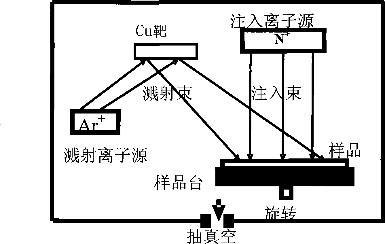
[0021] High-purity copper is selected as the target material, and it is fixed on a square target platform with special copper screws. During the sputtering process, circulating cooling water is used to cool the target material. Select the above sputtering target, while sputtering the copper target, and use pure N 2 or Ar:N 2 The mixed ion beam produced by the 1:5 mixed high-purity gas bombards the deposited film. The accelerating voltage of the implanted ion beam is 10kV, and the beam intensity is 1mA. The damage effect of high-dose ion implantation breaks the Cu bond; the implanted N+ combines with Cu to form a cubic anti-ReO 3 Type crystal structure of high resistivity Cu 3 N film. The nitrogen or argon / nitrogen mixed beam generated by the bombardment ion source has a beam diameter greater than 150mm and a non-uniformity less than 15%. Uniform, highly oriented Cu 3 N polycrystalline structure.
[0022] The ion beam enhanced deposition copper nitride film prepared by th...
Embodiment 2
[0024] 99.99% high-purity copper is selected as the target material, fixed on a square target platform with special copper screws, and the target material is cooled by circulating cooling water during the sputtering process. Select the above sputtering target, while sputtering the copper target, and use pure N 2 or Ar:N 2 The mixed ion beam generated by the 1:5 mixed high-purity gas bombards the deposited film. The accelerating voltage of the implanted ion beam is 30kV, and the beam current intensity is 2mA. The damage effect of high-dose ion implantation breaks Cu bonds; implanted N + Combined with Cu to form a cubic anti-ReO 3 Type crystal structure of high resistivity Cu 3 N film. The nitrogen or argon / nitrogen mixed beam generated by the bombardment ion source has a beam diameter greater than 150mm and a non-uniformity less than 15%. Uniform, highly oriented Cu 3 N polycrystalline structure.
[0025] The ion beam enhanced deposition copper nitride film prepared by t...
Embodiment 3
[0027] High-purity copper is selected as the target material, and it is fixed on a square target platform with special copper screws. During the sputtering process, circulating cooling water is used to cool the target material. Select the above sputtering target, while sputtering the copper target, and use pure N 2 or Ar:N 2 The mixed ion beam generated by the 1:5 mixed high-purity gas bombards the deposited film. The accelerating voltage of the implanted ion beam is 50kV, and the beam intensity is 4mA. The damage effect of high-dose ion implantation breaks Cu bonds; implanted N + Combined with Cu to form a cubic anti-ReO 3 Type crystal structure of high resistivity Cu 3 N film. The nitrogen or argon / nitrogen mixed beam generated by the bombardment ion source has a beam diameter greater than 150mm and a non-uniformity less than 15%. Uniform, highly oriented Cu 3 N polycrystalline structure.
[0028] The ion beam enhanced deposition copper nitride film prepared by the ab...
PUM
| Property | Measurement | Unit |
|---|---|---|
| electrical resistivity | aaaaa | aaaaa |
Abstract
Description
Claims
Application Information
 - R&D
- Intellectual Property
- Life Sciences
- Materials
- Tech Scout
- Unparalleled Data Quality
- Higher Quality Content
- 60% Fewer Hallucinations
Browse by: Latest US Patents, China's latest patents, Technical Efficacy Thesaurus, Application Domain, Technology Topic, Popular Technical Reports.
© 2025 PatSnap. All rights reserved.Legal|Privacy policy|Modern Slavery Act Transparency Statement|Sitemap|About US| Contact US: help@patsnap.com