
Apparatus for implementing non-mask surface plasma interference photolithography by using Lloyd lens

A surface plasmon and interference lithography technology, applied in the field of nanofabrication, can solve the problems of increased production cost, high production cost, small processing area, etc., and achieves the effects of high work efficiency, low cost and large area

Inactive Publication Date: 2009-05-27
INST OF OPTICS & ELECTRONICS - CHINESE ACAD OF SCI
View PDF0 Cites 12 Cited by
  • Summary
  • Abstract
  • Description
  • Claims
  • Application Information

AI Technical Summary

Problems solved by technology

However, almost all substances in the extreme ultraviolet band will show completely different properties from those in the ultraviolet band, which requires the imaging system of extreme ultraviolet lithography to be re-established, which greatly increases the production cost
In addition, electron beam direct writing and focused ion beam direct writing, which work by point-by-point scanning, have high production costs, low work efficiency and small processing area, which limits their application in many fields.

Method used


Image

  • Apparatus for implementing non-mask surface plasma interference photolithography by using Lloyd lens

Examples


Embodiment Construction

[0027] The present invention will be described in detail below in conjunction with the accompanying drawings and specific embodiments. But the following examples are only limited to explain the present invention, and the protection scope of the present invention should include the whole content of claim, and promptly can realize the whole content of claim of the present invention to those skilled in the art through following embodiment.

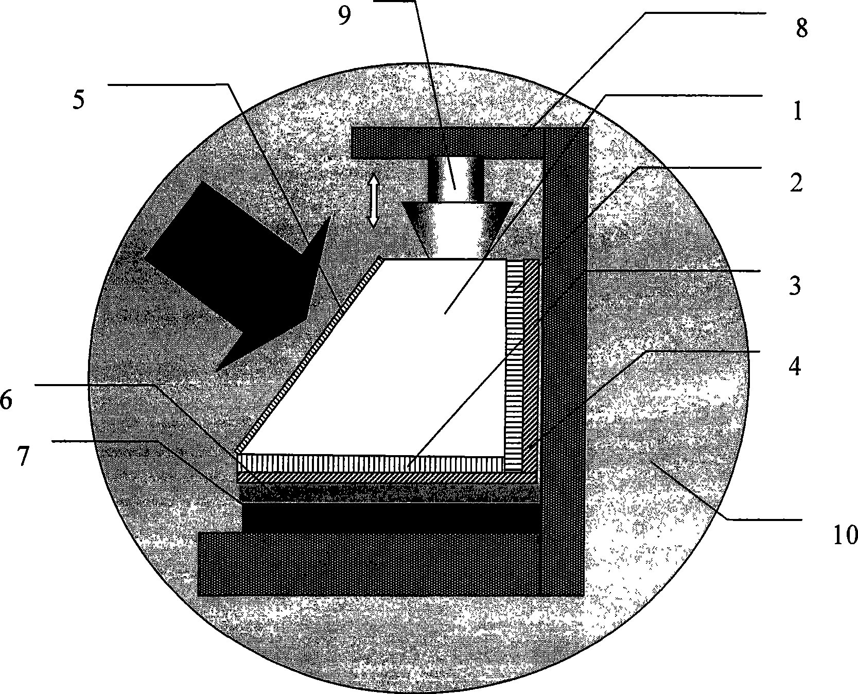
[0028] A device for realizing maskless surface plasmon interference lithography using a Lloyd mirror in this embodiment, its structural schematic diagram is as follows figure 1 As shown; including: a precision turntable 10 for adjusting the angle of incident light; a right-angled trapezoidal prism 1 for coupling excitation surface plasmon interference; a pressing device 9 for pressing the substrate 7 and the right-angled trapezoidal prism 1; Fix the support 8 of the pressing device 9 .

[0029] The right-angled trapezoidal prism in the devic...


PUM

PropertyMeasurementUnit
Thicknessaaaaaaaaaa
Thicknessaaaaaaaaaa
Thicknessaaaaaaaaaa

Abstract

The invention relates to a device of realizing the interference photolithography of a maskless surface plasma body through a laue mirror. The device comprises a precision turntable capable of adjusting the incident light angle, a rectangular dove prism capable of coupling and exciting the surface plasma body interference, a compressing device capable of compressing a substrate and the rectangular dove prism, and a support capable of fixing the compressing device. One side face of the rectangular dove prism is fixed on the precision turntable; a P polarized laser beam reaches the inclined plane in a mode of vertical incidence; and the precision turntable is adjusted finely to determine the real resonance angle for exciting the surface plasma body. The substrate coated with photoresist is arranged on the bottom surface of the prism; and the compressing device is adjusted so as to compress the prism and the substrate. A wide beam reaches the prism in a mode of incidence with the real resonance angle; and the surface plasma body interference and the exposure of the photoresist can be realized on the lower surface of a metal membrane; and the substrate after exposure is taken off. The surface plasma body interference photolithography is realized after the postbaking and development of the photoresist. The device has the advantages of low cost, high working efficiency, a great area of a processed pattern region, convenient assembly and adjustment, and the like. The device also facilitates the study and application of nanometer photon crystals and artificial materials.

Description

technical field [0001] The invention belongs to the technical field of nanometer processing, and relates to a device for realizing surface plasmon interference lithography. technical background [0002] With the continuous and in-depth development of nanofabrication technology, various nanophotonic devices, especially periodic nanostructures such as nanogratings and nanophotonic crystals, have gradually been widely concerned and applied in practice. For example, nano-gratings can be applied to high-precision measurement sensing and high-density storage, and nano-photonic crystals can be used as artificial materials to achieve functions such as negative refraction, super-resolution, and high-sensitivity biosensing. [0003] Since traditional photolithography is limited by the diffraction limit, in order to fabricate smaller-sized nanostructures, shorter-wavelength light sources must be used. According to this principle, the main nanofabrication technologies currently being d...

Claims


Application Information

Patent Timeline
IPC IPC(8): G03F7/20G03F7/00
Inventor 方亮王长涛刘尧罗先刚
Owner INST OF OPTICS & ELECTRONICS - CHINESE ACAD OF SCI
Learn More