Method for preparing high-dielectric-coefficient grid medium membrane hafnium silicon oxygen nitrogen

A high dielectric constant, hafnium silicon oxygen nitrogen technology, which is applied in the manufacture of circuits, electrical components, semiconductor/solid state devices, etc., can solve the problems of increased power consumption and increased leakage of gate dielectrics, and achieves low leakage current and good interface. , the effect of low cost

Inactive Publication Date: 2009-06-03
INST OF MICROELECTRONICS CHINESE ACAD OF SCI
View PDF0 Cites 18 Cited by
  • Summary
  • Abstract
  • Description
  • Claims
  • Application Information

AI Technical Summary

Problems solved by technology

[0010] In view of this, the main purpose of the present invention is to provide a method for preparing high dielectric constant gate dielectric thin film HfSiON, to solv

Method used


Image

  • Method for preparing high-dielectric-coefficient grid medium membrane hafnium silicon oxygen nitrogen
  • Method for preparing high-dielectric-coefficient grid medium membrane hafnium silicon oxygen nitrogen
  • Method for preparing high-dielectric-coefficient grid medium membrane hafnium silicon oxygen nitrogen

Examples


Embodiment Construction

[0036] In order to make the object, technical solution and advantages of the present invention clearer, the present invention will be described in further detail below in conjunction with specific embodiments and with reference to the accompanying drawings.

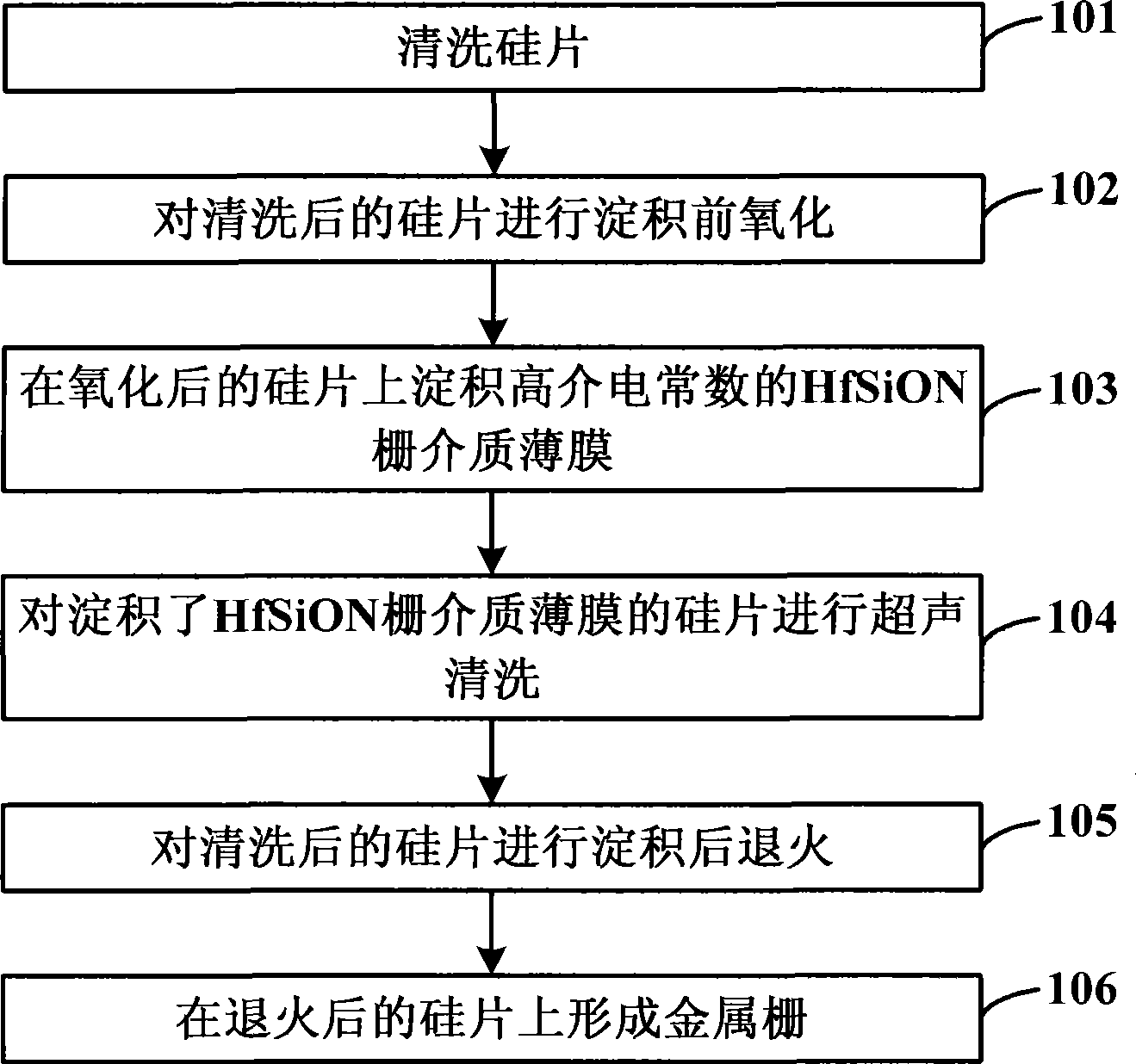
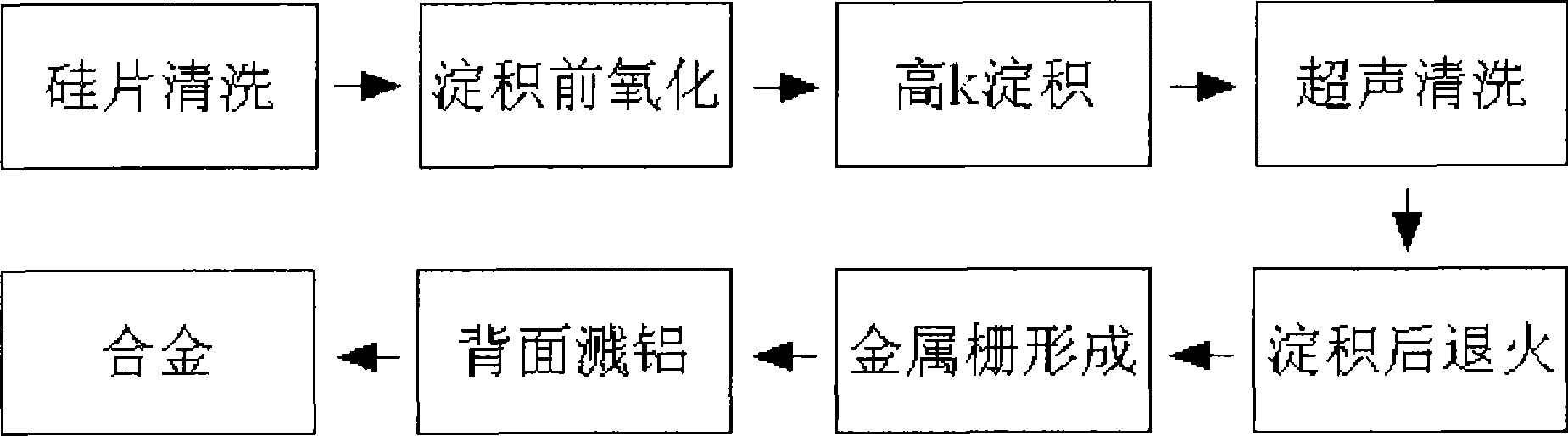
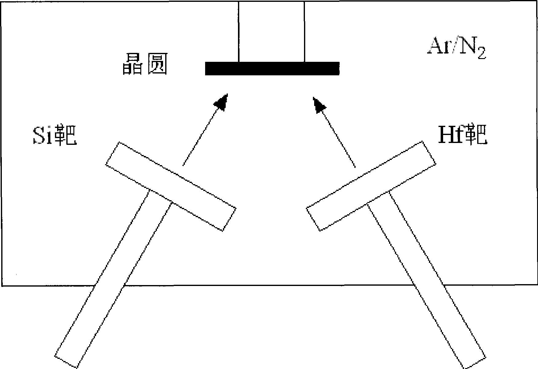
[0037] The present invention adopts the magnetron sputtering process to prepare hafnium silicon oxygen nitrogen (HfSiON) high dielectric constant gate dielectric film. Alcohol / water solution soaked at room temperature, rinsed with deionized water, put into the furnace immediately after drying, grew the interface layer by rapid thermal annealing, and used magnetron sputtering technology to alternately sputter hafnium ( Hf) target and silicon (Si) target are deposited to form HfSiON high dielectric constant gate dielectric film. After deposition, rapid thermal annealing is performed to complete the HfSiON high dielectric constant gate dielectric film, and then metal gate electrodes are formed for electrical measurement.

[...


PUM


Abstract

The invention discloses a method for preparing high-dielectric-coefficient grid medium membrane HfSiON, comprising the following steps: a silicon slice is washed; the washed silicon slice is oxidized before deposition; a high-dielectric-coefficient HfSiON grid medium membrane is deposited on the oxidized silicon slice; ultrasound washing is carried out on the silicon slice of the deposited HfSiON grid medium membrane; annealing is carried out on the washed silicon slice after deposition; and a metal grid is formed on the annealed silicon slice. The method can be used for solving the problems of sharp rise of grid medium leakage and acute increase of power consumption caused by thickness reduction of grid medium of small-sized apparatus.

Description

technical field [0001] The present invention relates to the technical field of nanometer feature size semiconductor device preparation, in particular to a method for preparing a high dielectric constant gate dielectric film hafnium silicon oxide nitride (HfSiON) used in the manufacture of nanoscale complementary metal oxide semiconductor devices to solve the problem of With the thinning of the gate dielectric thickness of small-scale devices, the leakage of the gate dielectric rises sharply and the power consumption increases seriously. Background technique [0002] For more than 40 years, integrated circuit technology has continued to develop according to Moore's law, with continuous shrinking of feature size, continuous improvement of integration, and increasingly powerful functions. As the device size continues to decrease, the thickness of the gate oxide layer decreases accordingly. [0003] At present, the characteristic size of metal oxide semiconductor transistors (M...

Claims


Application Information

Patent Timeline
IPC IPC(8): H01L21/28H01L21/336
Inventor 许高博徐秋霞柴淑敏
Owner INST OF MICROELECTRONICS CHINESE ACAD OF SCI
Why Eureka
Try Eureka