Boiling enhanced heat exchange structure of chips and fabrication method thereof

A technology that enhances heat transfer and manufacturing methods. It is applied in semiconductor/solid-state device manufacturing, electrical components, and electrical solid-state devices. It can solve problems such as high superheat, not obvious improvement effect, and thermal shock of chips, so as to overcome critical heat flow. The effect that the density improvement effect is not obvious

Inactive Publication Date: 2009-06-03
XI AN JIAOTONG UNIV
View PDF1 Cites 18 Cited by
  • Summary
  • Abstract
  • Description
  • Claims
  • Application Information

AI Technical Summary

Problems solved by technology

From the beginning of boiling to the state of critical heat flux, the temperature of the heating surface hardly increases with the increase of heat flux, which makes up for the deficiency of the surface microstructure developed by previous researchers, but there are the following problems: one is that it takes a long time for boiling to start. High wall superheat, and second, there is an obvious temperature jump process from the beginning of boiling to nucleate boiling heat transfer, resulting in thermal shock to the chip
Rece

Method used


Image

  • Boiling enhanced heat exchange structure of chips and fabrication method thereof
  • Boiling enhanced heat exchange structure of chips and fabrication method thereof
  • Boiling enhanced heat exchange structure of chips and fabrication method thereof

Examples


Embodiment

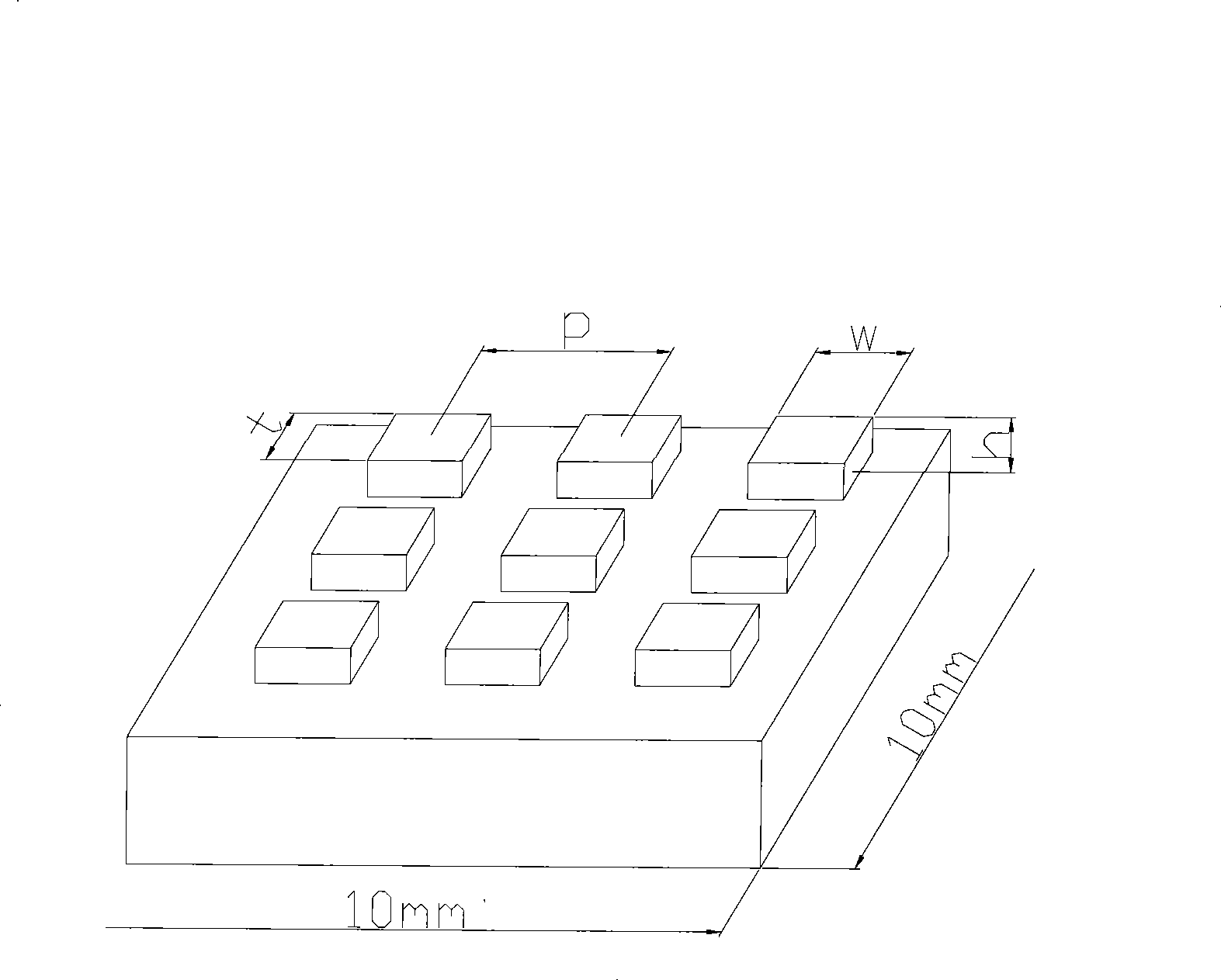
[0032] The manufacturing method of the boiling enhanced heat transfer structure of the chip of the present invention, the boss is a square columnar structure, the size is 50 μm×50 μm×60 μm (w×t×h), and the center pitch p is 100 μm. The specific manufacturing steps are as follows:

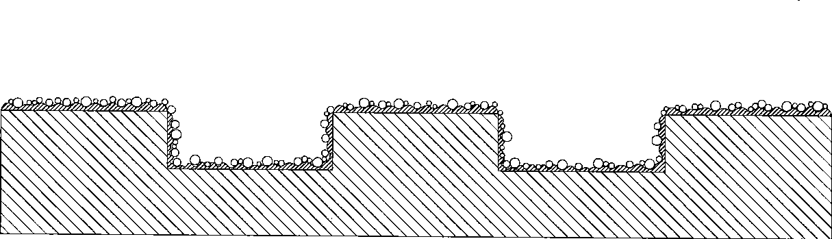
[0033] Step 1: Using a dry etching process, process bosses with columnar structures with the same size and uniform spacing on the surface of the chip. Specifically, a silicon wafer with a size of 10mm×10mm is cut from phosphorus-doped N-type semiconductor single crystal silicon with a thickness of 0.5mm and a diameter of 150mm as chips. Apply photoresist on the surface of the chip to form a photoresist film; make a mask whose size is consistent with the boss structure; then, use exposure technology to photoetch the photoresist film to form a pattern corresponding to the size of the boss photoresist pattern; finally, using dry etch gas Cl 2 Etching is performed until the boss height is 60 μm. Corro...


PUM

PropertyMeasurementUnit
Heightaaaaaaaaaa
Diameteraaaaaaaaaa
Thicknessaaaaaaaaaa

Abstract

The invention relates to a high heat flux density boiling enhanced heat exchange technology, in particular to amicroelectronic chip high efficiency cooling technology with a high heat flux density, particularly the boiling enhanced heat exchange structure of chips and the fabrication method thereof, which is characterized in that a plurality of lug bosses with a column structure are corroded on the surface of a chip; a SiO2 layer is splashed on the surface of the chip with the lug bosses; and the SiO2 layer is corroded to form a porous structure. The boiling enhanced heat exchange structure of chips can provide sufficient bubble nucleation number and a larger effective heat exchange area under the circumstance of a lower wall surface superheat degree, thereby solving the problem that the thermal shock of the chip exists from incipient boiling to nucleate boiling, and meanwhile, improving critical heat flux density remarkably to ensure the effective heat exchange of a high heat flux density electronic device.

Description

technical field [0001] The invention relates to a high heat flux boiling enhanced heat transfer technology, in particular to a high heat flux density microelectronic chip efficient cooling technology, specifically a chip boiling enhanced heat transfer structure and a manufacturing method thereof. Background technique [0002] With the rapid development of microelectronics technology, electronic products tend to develop in the direction of high performance, portability and miniaturization. The continuous reduction of the feature size of electronic devices and the continuous improvement of chip integration and circuit operating frequency have led to a rapid increase in chip heat flux, which has become the primary problem restricting the development of highly integrated chip technology. It is estimated that in the near future, the heat flux density of the chip can be as high as 10 2 W / cm 2 Above, if the heat generated is not dissipated in time, the temperature of the chip wil...

Claims


Application Information

Patent Timeline
IPC IPC(8): H01L23/367H01L23/373H01L23/44H01L21/00H01L21/311
CPCH01L2924/0002
Inventor 魏进家薛艳芳方嘉宾高秀峰袁敏哲
Owner XI AN JIAOTONG UNIV
Why Eureka
Try Eureka