Method for preparing gallium nitride based field-effect transistor

A gallium nitride-based field and gallium nitride-based technology, which is applied in the field of manufacturing gallium nitride-based field effect transistors, can solve the problems of AlGaN surface pollution and increase of AlGaN surface state density, and achieve surface state elimination, suppression increase, The effect of solving the current collapse effect

Active Publication Date: 2010-04-14
中科芯未来微电子科技成都有限公司
View PDF5 Cites 3 Cited by
  • Summary
  • Abstract
  • Description
  • Claims
  • Application Information

AI Technical Summary

Problems solved by technology

[0019] Another object of the present invention is to provide a method for manufacturing a GaN-based field effect transistor to solve the problem of AlGaN surface contamination caused by carbon and oxygen caused by long-term exposure of the AlGaN surface in the air, and the increase of the AlGaN surface state density, thereby Effective suppression of AlGaN / GaN HEMT current collapse effect

Method used


Image

  • Method for preparing gallium nitride based field-effect transistor
  • Method for preparing gallium nitride based field-effect transistor
  • Method for preparing gallium nitride based field-effect transistor

Examples


Embodiment Construction

[0047] In order to make the object, technical solution and advantages of the present invention clearer, the present invention will be described in further detail below in conjunction with specific embodiments and with reference to the accompanying drawings.
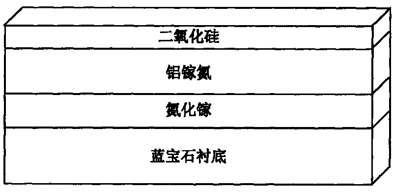
[0048] The core idea of ​​the present invention is to use a mixed solution of acetone, isopropanol, hydrochloric acid and hydrofluoric acid to treat the surface of gallium nitride-based materials, remove surface dirt, corrode the original oxide layer on the surface, and eliminate surface damage caused by the oxide layer. state, which reduces the surface state density of gallium nitride-based materials, and before the HEMT manufacturing process, PECVD is the first to deposit silicon dioxide on gallium nitride-based materials to protect the surface of gallium nitride-based materials and avoid gallium nitride-based materials. The surface of the material is exposed in the air, which prevents the surface of the gallium nitride-...


PUM


Abstract

The invention discloses a method of manufacturing GaN-based field-effect transistors, which includes steps of surface-finishing a GaN-based material layer, depositing a silicon oxide protective layer,forming lithographic alignment marks via lithography, dry-etching the silicon oxide protective layer, evaporating marked metal, forming source-drain patterns via lithography, dry-etching the siliconoxide protective layer, evaporating source-drain metal, annealing alloy at high temperature, forming shielding active region patterns via lithography, forming active region isolation via ion implantation, then wet-etching the silicon oxide protective layer, depositing silicon nitride on the surface of the GaN-based material, passivating field effect transistors, forming grids via electron-beam direct writing or optical lithography, dry-etching the silicon nitride and the GaN-based material layer at the top to form a gate-recessed structure, evaporating gate metal and metal wiring. The method of manufacturing GaN-based field-effect transistors avoids the surface of the GaN-based material being exposed in air, prevents the surface of the GaN-based material from being polluted during fabrication process, and inhibits current collapse effect of AlGaN / GaN HEMTs.

Description

technical field [0001] The invention relates to the technical field of wide-bandgap semiconductor material field effect transistors (FETs), in particular to a method for manufacturing gallium nitride (GaN)-based field effect transistors. Background technique [0002] As the third-generation wide-bandgap semiconductor material, GaN has a large bandgap (3.4eV), a high breakdown voltage (3.3MV / cm), a high concentration of two-dimensional electron gas (>1013cm2), and a large saturated electron velocity (2.8 X107cm / s) and other characteristics have received extensive attention internationally. At present, the high frequency, high voltage, high temperature and high power characteristics of AlGaN / GaN HEMT devices make them have great prospects in microwave power devices. [0003] For conventional GaN HEMT devices for X-band, the usual process steps are: [0004] Step 1. Electron beam direct writing lithography or ordinary optical lithography to form an electron beam alignment ...

Claims


Application Information

Patent Timeline
Patent Type & Authority Patents(China)
IPC IPC(8): H01L21/335
Inventor 李诚瞻魏珂郑英奎刘果果和致经刘新宇刘键
Owner 中科芯未来微电子科技成都有限公司
Why Eureka
Try Eureka